EM78P341N/342N/343N
8-Bit Microprocessor with OTP ROM
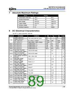
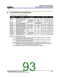
Symbol
Parameter
Condition
VOL = GND+0.5V
Min
Typ
10
15
-75
Max
Unit
Output Low Voltage
(Ports 5, P60~66, P70)
IOL1
−
−
mA
Output Low Voltage
(IR OUT (Port 67))
IOL2
VOL = GND+0.5V
−
−
mA
IPH
IPL
Pull-high current
Pull-low current
Pull-high active, input pin at VSS
Pull-low active, input pin at Vdd
-70
35
-80
45
µA
µA
40
All input and I/O pins at VDD,
output pin floating, WDT disabled
ISB1
ISB2
Power down current
Power down current
−
−
1.0
2.0
10
µA
µA
All input and I/O pins at VDD,
output pin floating, WDT enabled
6.0
15
Operating supply current
at two clocks (VDD to
3V)
/RESET= 'High', Fosc=32kHz
(Crystal type,CLKS="0"), output
pin floating, WDT disabled
ICC1
ICC2
ICC3
ICC4
−
−
−
−
20
25
µA
µA
Operating supply current
at two clocks (VDD to
3V)
/RESET= 'High', Fosc=32kHz
(Crystal type,CLKS="0"), output
pin floating, WDT enabled
15
1.9
3.0
/RESET= 'High', Fosc=4MHz
(Crystal type, CLKS="0"), output
pin floating, WDT enabled
Operating supply current
at two clocks
2.2
3.5
mA
mA
/RESET= 'High', Fosc=10MHz
(Crystal type, CLKS="0"), output
pin floating, WDT enabled
Operating supply current
at two clocks
Note: 1. These parameters are hypothetical (not tested) and are provided for design reference use only.
2. Data under minimum, typical, & maximum (Min, Typ, & Max) columns are based on hypothetical results at 25°C. These
data are for design reference only.
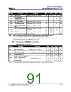
8.1 AD Converter Characteristics
Vdd=2.5V to 5.5V, Vss=0V, Ta=25°C
Symbol
VAREF
VASS
Parameter
Condition
Min.
2.5
Typ.
–
Max.
Vdd
Vss
Unit
V
Analog reference voltage VAREF - VASS ≥ 2.5V
Vss
VASS
750
–10
500
200
–
V
VAI
Analog input voltage
Analog supply current
–
–
VAREF
1000
+10
V
Ivdd
IAI1
850
0
uA
uA
uA
uA
Vdd=VAREF=5.0V, VASS =0.0V
(V referenced from Vdd)
Ivref
Ivdd
IAI2
600
250
820
Vdd=VAREF=5.0V, VASS=0.0V
(V referenced from VREF)
Analog supply current
OP current
IVref
300
Vdd=5.0V, OP used
IOP
450
550
650
uA
Output voltage swing 0.2V to 4.8V
RN
LN
Resolution
Vdd=VAREF=5.0V, VASS =0.0V
10
0
11
±4
–
Bits
°
Linearity error
Vdd = 2.5 to 5.5V Ta=25 C
±8
LSB
Differential nonlinear
error
°
DNL
FSE
Vdd = 2.5 to 5.5V Ta=25 C
0
±0.5
±4
±0.9
±8
LSB
LSB
Full scale error
Vdd=VAREF=5.0V, VASS =0.0V
±0
84 •
Product Specification (V1.0) 12.01.2006
(This specification is subject to change without further notice)

 ELAN [ ELAN MICROELECTRONICS CORP ]