EM78P312N
8-Bit Microcontroller
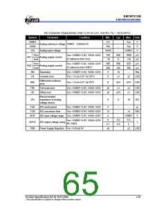
Ta= 25 °C, VDD= 3.0V 5%, VSS= 0V
Symbol
Parameter
Condition
Min.
Typ.
Max.
Unit
Fc
Crystal: 2.5V to VDD
ERC: VDD = 3V
Two cyclea with two clocks
1
−
850
4
MHz
kHz
ERC
R: 5.1KΩ, C: 100 pF
600
1100
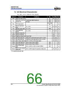
Input High Threshold
Voltage (Schmitt Trigger)
Sink current
VIHRC
IRC1
VILRC
IRC2
IIL
OSCI in RC mode
VI from low to high , VI=5V
OSCI in RC mode
1.6
7
2.3
9.5
1
2.8
12
1.3
11
1
V
μA
V
Input Low Threshold
Voltage (Schmitt Trigger)
Sink current
0.7
6
VI from high to low , VI=2V
VIN = VDD, VSS
8.5
0
μA
μA
Input Leakage Current for
input pins
-1
Input High Voltage
(Schmitt Trigger)
Input Low Voltage
(Schmitt Trigger)
Input High Threshold
Voltage (Schmitt Trigger)
Input Low Threshold
Voltage (Schmitt Trigger)
Clock Input High Voltage
Clock Input Low Voltage
Output High Voltage
(Ports 6, 7, 8, 9)
VIH1
VIL1
Ports 6,7,8,9,A
Ports 6,7,8,9,A
/RESET, TCC
/RESET, TCC
0.7VDD
-0.3V
−
−
−
−
VDD+0.3V
0.3VDD
V
V
V
V
VIHT2
VILT2
0.7 VDD
-0.3V
VDD +0.3V
0.3 VDD
VIHX1
VILX1
LOSCI, OSCI in crystal mode
LOSCI, OSCI in crystal mode
0.7 VDD
-0.3V
−
−
VDD +0.3V
0.3 VDD
V
V
IOH1
IOL1
IOL2
VOH = VDD-0.4V
VOL = VSS+0.4V
VOL = VSS+0.4V
-2
2
-3.5
3.5
13
-5
5
mA
mA
mA
Output Low Voltage
(Port 9)
Output Low Voltage
(Ports 6,Port7, Port8)
Pull-high current
10
16
IPH
IPL
Pull-high active, input pin at VSS
Pull-low active, input pin at VDD
-15
15
-23
23
-31
30
μA
μA
Pull-low current
Sleep mode
Power down current
Sleep mode
Power down current
Idle mode
ISB1
ISB2
All input and I/O WDT disabled
pins at VDD,
−
−
0.4
1.5
0.8
3
μA
μA
output pin floating
WDT enabled
ICC3
ICC4
Operating supply current
at two clocks
−
−
0.3
1.1
0.5
1.5
mA
mA
VDD=3V, /RESET= 'High',
Fc=4MHz, CLKS="0", output pin
floating, WDT enabled
Normal mode
Operating supply current
at two clocks
Note: * Data in the Minimum, Typical, Maximum (“Min”, “Typ”, ”Max”) columns are based on characterization results at 25°C.
60 •
Product Specification (V1.0) 10.03.2006
(This specification is subject to change without further notice)

 ELAN [ ELAN MICROELECTRONICS CORP ]