A Product Line of
Diodes Incorporated
ZXCT1107/1109/1110
LOW POWER HIGH-SIDE CURRENT MONITORS
Application Information (cont.)
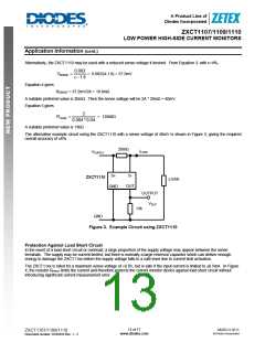
Figure 4. Protection and EMC Filtering
EMC Susceptibility
In many applications, the circuit is required to operate in the presence of RF radiation. This radiation is coupled into the
circuit via the supply or load connections and will often cause significant bias shift due to rectification within the integrated
circuit. The bias shift may lead to erroneous operation of the integrated circuit. In Figure 4, a low pass filter, RPROT and C1,
provides significant attenuation in the VHF and UHF regions. The value of C1 is recommended to be in the range of 10pF to
47pF, leadless ceramic type.
PCB Layout Considerations
It is necessary to take into account a small volt drop in the PCB copper and solder joints to RSENSE. Such volt drops can
create noticeable error at currents of the order of 1A and greater. The PCB must be designed to provide the maximum
possible copper carrying current via the sense resistor, and the traces from the S+ and S- pins must be connected only to the
resistor pads. In this way, the effect of the copper is minimized.
If used, the capacitor C1 should be placed very close the input pins S+ and S-.
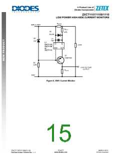
Application: High Voltage Current Monitor
The schematic of Figure 5 shows how the current monitor may be used in a high voltage application such as a TV LED
backlight system. In this configuration the 500V PNP transistor Q1 drops a large proportion of the supply voltage. Diode D2
limits the differential input voltage to a safe level under overload conditions. The voltage across U1 is limited by the zener
diode D1. The output current of U1 is limited to about 3mA by the D2. As RGAIN is typically a few kΩ, the output voltage is
therefore limited to a few volts. An additional output clamping diode may be required for higher gains. R1 is chosen to
give a suitable bias current in D1 for the given supply voltage range.
14 of 17
www.diodes.com
MARCH 2011
© Diodes Incorporated
ZXCT1107/1109/1110
Document number: DS35033 Rev. 1 - 2

 DIODES [ DIODES INCORPORATED ]