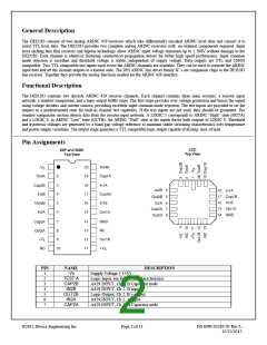
PIN
8
9
NAME
OUT2A
+VL
DESCRIPTION
Logic Output, Ch 2, A’s output
Supply Voltage (+5V)
10
11
12
13
14
15
16
17
18
19
20
NC
+VS
OUT1B
NC
GND
OUT1A
IN1B
CAP1B
IN1A
CAP1A
TESTB
Supply Voltage (+15V)
Logic Output, Ch 1, B’s output
Supply Return
Logic Output, Ch 1, A’s output
A429 INPUT, Ch 1, B input
A429 INPUT, Ch 1, B Capacitor node
A429 INPUT, Ch 1, A input
A429 INPUT, Ch 1, A Capacitor node
Logic Input, see functional characteristics.
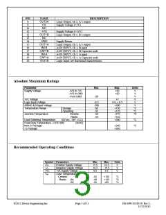
Absolute Maximum Ratings
Parameter
Supply Voltage:
Min.
Max.
+36
+20
Units
V
V
+VS to -VS
+VS to GND
-Vs to GND
-20
V
+VL Voltage
+7
+VL + 0.3
+200
+150
+125
V
V
V
°C
°C
°C
Logic Input Voltage
ARINC 429 Input Voltage
Temperature Range
-0.3
-200
-65
-55
-55
Storage
Operating
Ceramic
Junction Temperature
+175
Plastic
-55
+145
Lead Soldering Temperature
Peak Body Temperature, J-STD-020
Non-G Package
(60 sec., DIP, LCC)
+300
°C
°C
(SOIC)
+240
+260
-G Package
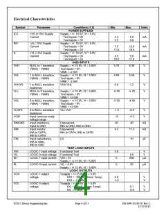
Recommended Operating Conditions
Symbol Parameters
Min.
Max.
16.5
-13.5
5.5
Units
+Vs
-Vs
+VL
Top
Positive Supply Voltage
Negative Supply Voltage
+VL Supply Voltage
Case Temperature
Ceramic
13.5
-16.5
4.5
V
V
V
-55
-40
-55
+125
+125
+85
°C
°C
°C
Plastic: -SA
-SE
©2012 Device Engineering Inc
Page 3 of 11
DS-MW-03283-01 Rev L
12/12/2012

 DEIAZ [ Device Engineering Incorporated ]