General Description
The DEI3283 consists of two analog ARINC 429 receivers which take differentially encoded ARINC level data and convert it to
serial TTL level data. The DEI3283 provides two complete analog ARINC receivers with no external components required. Input
level shifting thin film resistors and bipolar technology allow ARINC input voltage transients up to rꢀ200V without damage to the
DEI3283. Each channel is identical, featuring symmetrical propagation delays for better high speed performance. Input common
mode rejection is excellent and threshold voltage is stable, independent of supply voltage. Data outputs are TTL and CMOS
compatible. Two TTL compatible test inputs used to test the ARINC channels are available. They can be used to override the ARINC
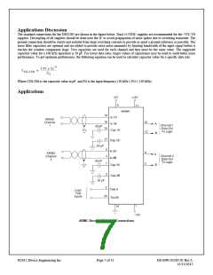
input data and set the channel outputs to a known state. The DEI ARINC line driver family IC’s are companion chips to the DEI3283
line receiver. Together they provide the analog functions needed for the ARINC 429 interface.
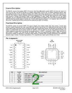
Functional Description
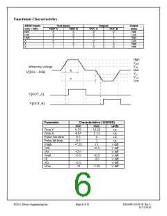
The DEI3283 contains two discrete ARINC 429 receiver channels. Each channel contains three main sections: a resistor input
network, a window comparator, and a logic output buffer stage. The first stage provides over voltage protection and biases the signal
using voltage dividers and current sources, providing excellent input common mode rejection. The test inputs are provided to set the
outputs to a predetermined state for built-in channel test capability. If the test inputs are not used, they should be grounded. The
window comparator section detects data from the resistor input network. A LOGIC 1 corresponds to ARINC “High” state (OUTA)
and a LOGIC 0, to ARINC “Low” state (OUTB). An ARINC “Null” state at the inputs forces both outputs to LOGIC 0. Threshold
and hysteresis voltages are generated by a band gap voltage reference to maintain stable switching characteristics over temperature
and power supply variations. The output stage generates a TTL compatible logic output capable of driving 3mA of load.
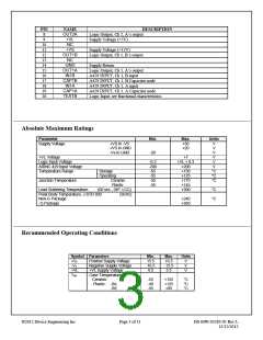
Pin Assignments
PIN
1
NAME
-Vs
DESCRIPTION
Supply Voltage (-15V)
2
3
4
Logic Input, see functional characteristics.
A429 INPUT, Ch 2, B Capacitor node
A429 INPUT, Ch 2, B input
TEST A
CAP2B
IN2B
5
6
Logic Output, Ch 2, B’s output
A429 INPUT, Ch 2, A input
OUT2B
IN2A
7
A429 INPUT, Ch 2, A Capacitor node
CAP2A
©2012 Device Engineering Inc
Page 2 of 11
DS-MW-03283-01 Rev L
12/12/2012

 DEIAZ [ Device Engineering Incorporated ]