DS3251/DS3252/DS3253/DS3254
9.4 Waveshaping, Line Build-Out, Line Driver
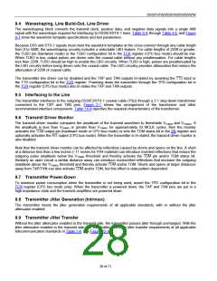
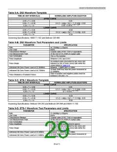
The waveshaping block converts the transmit clock, positive data, and negative data signals into a single AMI
signal with the waveshape required for interfacing to DS3/E3/STS-1 lines. Table 9-A through Table 9-E and Figure
9-1 show the waveform template specifications and test parameters.
Because DS3 and STS-1 signals must meet the waveform templates at the cross-connect through any cable length
from 0 to 450ft, the waveshaping circuitry includes a selectable LBO feature. For cable lengths of 225ft or greater,
the TLBO pin (hardware mode) or the TLBO configuration bit in the TCR register (CPU bus mode) should be low.
When TLBO is low, output pulses are driven onto the coaxial cable without any preattenuation. For cable lengths
less than 225ft, TLBO should be high to enable the LBO circuitry. When TLBO is high, pulses are preattenuated by
the LBO circuitry before being driven onto the coaxial cable. The LBO circuitry provides attenuation that mimics the
attenuation of 225ft of coaxial cable.
The transmitter line driver can be disabled and the TXP and TXN outputs tri-stated by asserting the TTS input or
the TTS configuration bit in the TCR register. Powering down the transmitter through the TPD configuration bit in
the TCR register (CPU bus mode) also tri-states the TXP and TXN outputs.
9.5 Interfacing to the Line
The transmitter interfaces to the outgoing DS3/E3/STS-1 coaxial cable (75ꢀ) through a 2:1 step-down transformer
connected to the TXP and TXN pins. Figure 2-1 shows the arrangement of the transformer and other
recommended interface components. Table 14-A specifies the required characteristics of the transformer.
9.6 Transmit Driver Monitor
The transmit driver monitor compares the amplitude of the transmit waveform to thresholds VTXMIN and VTXMAX. If
the amplitude is less than VTXMIN or greater than VTXMAX for approximately 32 MCLK cycles, then the monitor
activates the TDM output pin (hardware mode or CPU bus mode) or sets the TDM status bit in the SR register and
optionally activates the INT output (CPU bus mode). When the transmitter is tri-stated, the transmit driver monitor is
also disabled.
Note that the transmit driver monitor can be affected by reflections caused by shorts and opens on the line. A short
at a distance less than a few inches (~11 inches for FR4 material) can introduce inverted reflections that reduce the
outgoing pulse amplitude below the VTXMIN threshold and thereby activate the TDM pin and/or TDM status bit.
Similarly an open circuit a similar distance away can introduce noninverted reflections that increase the outgoing
amplitude above the VTXMAX threshold and thereby activate TDM and/or TDM. Shorts and opens at larger distances
away from TXP/TXN can also activate TDM and/or TDM, but this effect is data-pattern dependent.
9.7 Transmitter Power-Down
To minimize power consumption when the transmitter is not being used, assert the TPD configuration bit in the
TCR register (CPU bus mode only). When the transmitter is powered down, the TXP and TXN pins are put in a
high-impedance state and the transmit amplifiers are powered down.
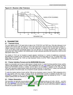
9.8 Transmitter Jitter Generation (Intrinsic)
The transmitter meets the jitter generation requirements of all applicable standards, with or without the jitter
attenuator enabled.
9.9 Transmitter Jitter Transfer
Without the jitter attenuator enabled in the transmit side, the transmitter passes jitter through unchanged. With the
jitter attenuator enabled in the transmit side, the transmitter meets the jitter transfer requirements of all applicable
telecommunication standards in Table 1-A. See Figure 10-1.
28 of 71

 DALLAS [ DALLAS SEMICONDUCTOR ]