DS2406
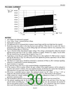
PIO SINK CURRENT
I
, I
SA
SB
100 mA
90 mA
80 mA
70 mA
60 mA
50 mA
40 mA
30 mA
20 mA
10 mA
@ 0.4V
max.
PIO-A
min.
max.
PIO-B
min.
V
PUP
2.8V
4V
5V
6V
NOTES:
1. All voltages are referenced to ground.
2. VPUP, VPUPA, VPUPB = external pull-up voltage.
3. Input load is to ground.
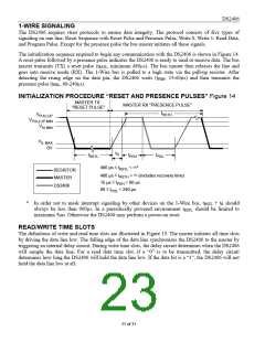
4. An additional reset or communication sequence cannot begin until the reset high time has expired.
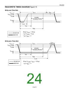
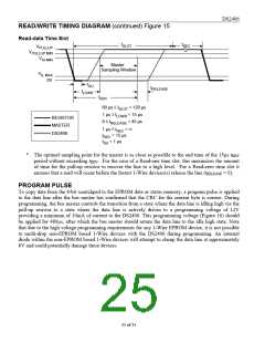
5. Read data setup time refers to the time the host must pull the 1-Wire bus low to read a bit. Data is
guaranteed to be valid within 1µs of this falling edge and will remain valid for 14µs minimum (15µs
total from falling edge on 1-Wire bus).
6. VIH is a function of the chip-internal supply voltage. This voltage is determined by either the external
pull-up resistor and VPUP or the VCC supply, whichever is higher. Without VCC supply, VIH for either
PIO pin should always be greater than or equal to VPUP -0.3V.
7. Capacitance on the data pin could be 800pF when power is first applied. If a 5kΩ resistor is used to
pull up the data line to VPUP, 5µs after power has been applied the parasite capacitance will not affect
normal communications.
8. The Reset Low Time (tRSTL) should be restricted to a maximum of 960μs to allow interrupt signaling;
otherwise, it could mask or conceal interrupt pulses.
9. Input resistance is to ground.
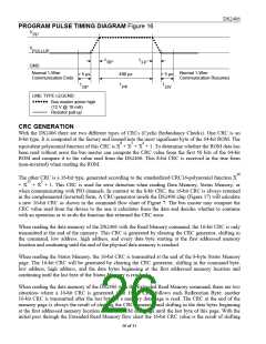
10. VCC must be at least 4.0V if it is to be connected during a programming pulse.
11. If the current at PIO-A reaches 200mA the gate voltage of the output transistor will be reduced to
limit the sink current to 200mA. The user-supplied circuitry should limit the current flow through the
PIO-transistor to no more than 100mA. Otherwise the DS2406 may be damaged.
12. PIO-A has a controlled turn-on output. The indicated currents are DC values. At VPUP = 4.0V or
higher the sink current typically reaches 80% of its DC value 1 µs after turning on the transistor.
13. Under certain low voltage conditions VILMAX may have to be reduced to as much as 0.5V to always
guarantee a presence pulse.
14. The accumulative duration of the programming pulses for each address must not exceed 5ms.
15. The optimal sampling point for the master is as close as possible to the end time of the 15μs tRDV
period without exceeding tRDV. For the case of a Read-one time slot, this maximizes the amount of
time for the pull-up resistor to recover the line to a high level. For a Read-zero time slot it ensures
that a read will occur before the fastest 1-Wire devices(s) release the line (tRELEASE = 0).
30 of 31

 DALLAS [ DALLAS SEMICONDUCTOR ]