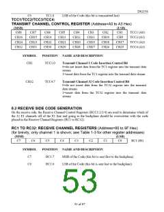
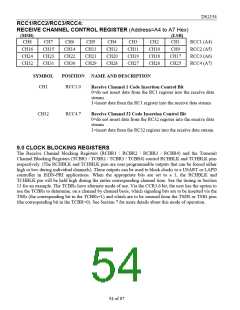
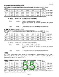
DS2154
11.0 ADDITIONAL (Sa) AND INTERNATIONAL (Si) BIT OPERATION
The DS2154 provides for access to both the Sa and the Si bits via three different methods. The first is via
a hardware scheme using the RLINK/RLCLK and TLINK/ TLCLK pins. The first method is discussed in
Section 11.1. The second involves using the internal RAF/RNAF and TAF/TNAF registers and is
discussed in Section 11.2 The third method which is covered in Section 11.3 involves an expanded
version of the second method and is one of the features added to the DS2154 from the original DS2153
definition.
11.1 HARDWARE SCHEME
On the receive side, all of the received data is reported at the RLINK pin. Via RCR2, the user can control
the RLCLK pin to pulse during any combination of Sa bits. This allows the user to create a clock that can
be used to capture the needed Sa bits. If RSYNC is programmed to output a frame boundary, it will
identify the Si bits. See Section 13 for detailed timing.
On the transmit side, the individual Sa bits can be either sourced from the internal TNAF register (see
Section 11.2 for details) or from the external TLINK pin. Via TCR2, the DS2154 can be programmed to
source any combination of the additional bits from the TLINK pin. If the user wishes to pass the Sa bits
through the DS2154 without them being altered, then the device should be set up to source all five Sa bits
via the TLINK pin and the TLINK pin should be tied to the TSER pin. Si bits can be inserted through the
TSER pin via the clearing of the TCR1.3 bit. Please see the timing diagrams and the transmit data flow
diagram in Section 13 for examples.
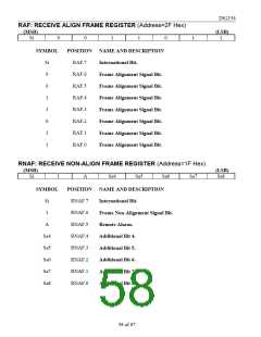
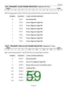
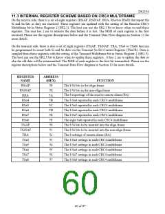
11.2 INTERNAL REGISTER SCHEME BASED ON DOUBLE-FRAME
On the receive side, the RAF and RNAF registers will always report the data as it received in the
Additional and International bit locations. The RAF and RNAF registers are updated with the setting of
the Receive Align Frame bit in Status Register 2 (SR2.6). The host can use the SR2.6 bit to know when to
read the RAF and RNAF registers. It has 250 us to retrieve the data before it is lost.
On the transmit side, data is sampled from the TAF and TNAF registers with the setting of the Transmit
Align Frame bit in Status Register 2 (SR2.3). The host can use the SR2.3 bit to know when to update the
TAF and TNAF registers. It has 250 us to update the data or else the old data will be retransmitted. Data
in the Si bit position will be overwritten if either the DS2154 is programmed: (1) to source the Si bits
from the TSER pin, (2) in the CRC4 mode, or (3) have automatic E-bit insertion enabled. Data in the Sa
bit position will be overwritten if any of the TCR2.3 to TCR2.7 bits are set to 1 (please see Section 11.1
for details). Please see the register descriptions for TCR1 and TCR2 and the Transmit Data Flow diagram
in Section 13 for more details.
57 of 87

 DALLAS [ DALLAS SEMICONDUCTOR ]