DS2154
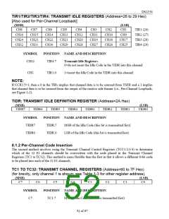
RCC1/RCC2/RCC3/RCC4:
RECEIVE CHANNEL CONTROL REGISTER (Address=A4 to A7 Hex)
(MSB)
(LSB)
CH8
CH7
CH15
CH23
CH31
CH6
CH14
CH22
CH30
CH5
CH13
CH21
CH29
CH4
CH12
CH20
CH28
CH3
CH11
CH19
CH27
CH2
CH10
CH18
CH26
CH1
RCC1 (A4)
CH16
CH24
CH32
CH9
CH17
CH25
RCC2 (A5)
RCC3 (A6)
RCC4 (A7)
SYMBOL
POSITION NAME AND DESCRIPTION
CH1
RCC1.0
RCC4.7
Receive Channel 1 Code Insertion Control Bit
0=do not insert data from the RC1 register into the receive data
stream
1=insert data from the RC1 register into the receive data stream
CH32
Receive Channel 32 Code Insertion Control Bit
0=do not insert data from the RC32 register into the receive data
stream
1=insert data from the RC32 register into the receive data stream
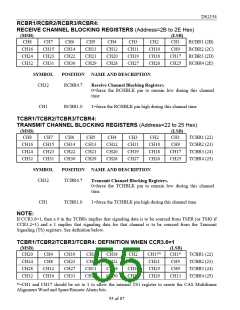
9.0 CLOCK BLOCKING REGISTERS
The Receive Channel blocking Registers (RCBR1 / RCBR2 / RCBR3 / RCBR4) and the Transmit
Channel Blocking Registers (TCBR1 / TCBR2 / TCBR3 / TCBR4) control RCHBLK and TCHBLK pins
respectively. (The RCHBLK and TCHBLK pins are user programmable outputs that can be forced either
high or low during individual channels). These outputs can be used to block clocks to a USART or LAPD
controller in ISDN-PRI applications. When the appropriate bits are set to a 1, the RCHBLK and
TCHBLK pin will be held high during the entire corresponding channel time. See the timing in Section
13 for an example. The TCBRs have alternate mode of use. Via the CCR3.6 bit, the user has the option to
use the TCBRs to determine, on a channel by channel basis, which signaling bits are to be inserted via the
TSRs (the corresponding bit in the TCBRs=1) and which are to be sourced from the TSER or TSIG pins
(the corresponding bit in the TCBR=0). See Section 7 for more details about this mode of operation.
54 of 87

 DALLAS [ DALLAS SEMICONDUCTOR ]