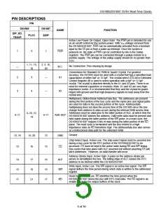
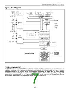
DS1685/DS1687 3V/5V Real-Time Clocks
POWER-DOWN/POWER-UP CONSIDERATIONS
The RTC function continues to operate, and all of the RAM, time, calendar, and alarm memory locations remain
nonvolatile regardless of the level of the VCC input. . At least one back up supply must remain within the minimum
and maximum limits whenever VCC is not at a valid level. When VCC is applied and exceeds VPF (power-fail trip
point), the device becomes accessible after tREC, provided that the oscillator is running and the oscillator countdown
chain is not in reset (Register A). This time period allows the system to stabilize after power is applied. If the
oscillator is not enabled, the oscillator enable bit will be enabled on power up, and the device becomes immediately
accessible.
The DS1685/DS1687 is available in either a 3V or a 5V device.
The 5V device is fully accessible and data can be written and read only when VCC is greater than 4.5V. When VCC
falls below VPF, read and writes are inhibited. However, the timekeeping function continues unaffected by the lower
input voltage. As VCC falls below the greater of VBAT and VBAUX, the RAM and timekeeper are switched over to a
lithium battery connected either to the VBAT pin or VBAUX pin.
The 3V device is fully accessible and data can be written or read only when VCC is greater than 2.7V. When VCC
falls below VPF, reads and writes are inhibited. If VPF is less than VBAT and VBAUX, the power supply is switched from
V
CC to the backup supply (the greater of VBAT and VBAUX) when VCC drops below VPF. If VPF is greater than VBAT and
BAUX, the power supply is switched from VCC to the backup supply when VCC drops below the larger of VBAT and
V
VBAUX
.
When VCC falls below VPF, the device inhibits access by internally disabling the CS input. With the possible
exception of the KS, PWR, and SQW pins, all inputs are ignored and all outputs are in a high-impedance state.
TIME, CALENDAR, AND ALARM LOCATIONS
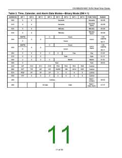
The time and calendar information is obtained by reading the appropriate register bytes shown in Table 2. The
time, calendar, and alarm are set or initialized by writing the appropriate register bytes. The contents of the time,
calendar, and alarm registers can be either binary or binary coded decimal (BCD) format. Table 2 shows the binary
and BCD formats of the 10 time, calendar, and alarm locations that reside in both bank 0 and in bank 1, plus the
two extended registers that reside in bank 1 only (bank 0 and bank 1 switching are explained later in this text).
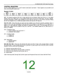
Before writing the internal time, calendar, and alarm registers, the SET bit in Register B should be written to a logic
1 to prevent updates from occurring while access is being attempted. Also at this time, the data format (binary or
BCD) should be set by the data mode bit (DM) of Register B. All time, calendar, and alarm registers must use the
same data mode. Invalid time and date entries will result in undefined operation. The set bit in Register B should
be cleared after the data mode bit has been written to allow the RTC to update the time and calendar bytes. If the
oscillator is running, the time and date registers will update 500ms after the countdown chain is enabled.
Once initialized, the RTC makes all updates in the selected mode. The data mode cannot be changed without
reinitializing the 10 data bytes. The 24/12 bit cannot be changed without reinitializing the hour locations. When the
12-hour format is selected, the high order bit of the hours byte represents PM when it is a logic 1. The time,
calendar, and alarm bytes are always accessible because they are double buffered. Once per second the 10 bytes
are advanced by one second and checked for an alarm condition
If a read of the time and calendar data occurs during an update, a problem exists where seconds, minutes, hours,
etc., might not correlate. The probability of reading incorrect time and calendar data is low. Several methods of
avoiding any possible incorrect time and calendar reads are covered later.
The three time alarm bytes can be used in two ways. First, when the alarm time is written in the appropriate hours,
minutes, and seconds alarm locations, the alarm interrupt is initiated at the specified time each day if the alarm
enable bit is high.
The second use condition is to insert a “don’t care” state in one or more of the three time-alarm bytes. The “don’t
care” code is any hexadecimal value from C0 to FF. The two most significant bits of each byte set the “don’t care”
condition when at logic 1. An alarm is generated each hour when the “don’t care” bits are set in the hours byte.
Similarly, an alarm is generated every minute with “don’t care” codes in the hours and minute alarm bytes. The
9 of 39

 DALLAS [ DALLAS SEMICONDUCTOR ]