DS1685/DS1687 3V/5V Real-Time Clocks
PIN DESCRIPTIONS
PIN
DS1685
DIP, SO,
TSSOP
DS1687
NAME
FUNCTION
PLCC
EDIP
Active Low Power-On Output, Open Drain. The PWR pin is intended for use
as an on/off control for the system power. With VCC voltage removed from
the DS1685/DS1687, PWR can be automatically activated from a kickstart
input by the KS pin or from a wake-up interrupt. Once the system is
powered on, the state of PWR can be controlled by bits in the Dallas
registers. The PWR pin can be connected through a pullup resistor to a
positive supply. The voltage of the pullup supply should be no greater than
5.5V.
1
2
1
PWR
1, 11, 13,
18
2, 3, 16,
20
No Connection. Pins missing by design.
—
2
N.C.
X1
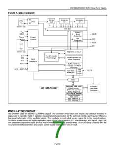
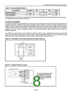
Connections for Standard 32.768kHz Quartz Crystal. For greatest
accuracy, the DS1685 must be used with a crystal that has a specified load
capacitance of either 6pF or 12.5pF. The crystal-select (CS) bit in Extended
Control Register 4B is used to select operation with a 6pF or 12.5pF
crystal. The crystal is attached directly to the X1 and X2 pins. There is no
need for external capacitors or resistors. Note: X1 and X2 are very high-
impedance nodes. It is recommended that they and the crystal be guard-
ringed with ground and that high-frequency signals be kept away from the
crystal area.
3
4
—
—
3
X2
Multiplexed, Bidirectional Address/Data Bus. The addresses are present
during the first portion of the bus cycle and the same pins and signal paths
are used for data in the second portion of the cycle. Address/data
multiplexing does not slow the access time of the DS1685 since the bus
change from address to data occurs during the internal RAM access time.
Addresses must be valid prior to the latter portion of ALE, at which time the
DS1685/DS1687 latches the address. Valid write data must be present and
held stable during the latter portion of the WR pulse. In a read cycle, the
DS1685/DS1687 outputs 8 bits of data during the latter portion of the RD
pulse. The read cycle is terminated and the bus returns to a high-
impedance state as RD transitions high. The address/data bus also serves
as a bidirectional data path for the extended RAM.
5–10, 12,
14
4–11
4–11
AD0–AD7
Ground
12, 16
13
15, 20
16
12
13
GND
Chip-Select Input, Active-Low. The chip-select signal must be asserted low
during a bus cycle for the RTC portion of the DS1685/DS1687 to be
accessed. CS must be kept in the active state during RD and WR timing.
Bus cycles that take place with ALE asserted but without asserting CS will
latch addresses. However, no data transfer will occur.
CS
Address-Strobe Input, Active High. A pulse on the address strobe pin
serves to demultiplex the bus. The falling edge of ALE causes the RTC
address to be latched within the DS1685/DS1687.
14
15
17
17
19
21
14
15
17
ALE
WR
RD
Write Input, Active Low. The WR signal is an active-low signal. The WR
signal defines the time period during which data is written to the addressed
register.
Read Input, Active Low. RD identifies the time period when the
DS1685/DS1687 drives the bus with RTC read data. The RD signal is an
enable signal for the output buffers of the clock.
5 of 39

 DALLAS [ DALLAS SEMICONDUCTOR ]