DS1685/DS1687 3V/5V Real-Time Clocks
LSB
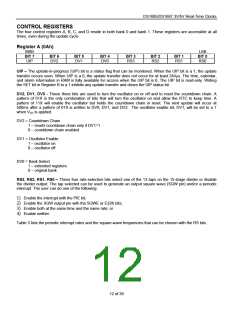
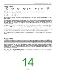
Register C (0Ch)
MSB
BIT 7
BIT 6
PF
BIT 5
BIT 4
BIT 3
BIT 2
BIT 1
BIT 0
IQRF
AF
UF
0
0
0
0
IRQF – The interrupt-request flag (IRQF) bit is set to a 1 when one or more of the following are true:
PF = PIE = 1
AF = AIE = 1
UF = UIE = 1
WF = WIE = 1
KF = KSE = 1
RF = RIE = 1
Any time the IRQF bit is a 1, the IRQ pin is driven low. Flag bits PF, AF, and UF are cleared after Register C is read
by the program.
PF – The periodic-interrupt flag (PF) is a read-only bit that is set to a 1 when an edge is detected on the selected
tap of the divider chain. The RS3–RS0 bits establish the periodic rate. PF is set to a 1 independently of the state of
the PIE bit. When both PF and PIE are 1’s, the IRQ signal is active and sets the IRQF bit. This bit may be cleared
by reading Register C.
AF – A 1 in the alarm-interrupt flag (AF) bit indicates that the current time has matched the alarm time. If the AIE bit
is also a 1, the IRQ pin goes low and a 1 appears in the IRQF bit. This bit may be cleared by reading Register C.
UF – The update-ended interrupt flag (UF) bit is set after each update cycle. When the UIE bit is set to 1, the one in
UF causes the IRQF bit to be a 1, which asserts the IRQ pin. This bit may be cleared by reading Register C.
BIT 3, BIT2, BIT 1, BIT 0 - These are unused bits of the status Register C. These bits always read 0 and cannot be
written.
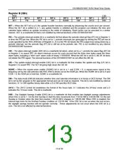
Register D (0Dh)
MSB
BIT 7
VRT
LSB
BIT 0
0
BIT 6
BIT 5
BIT 4
BIT 3
BIT 2
BIT 1
0
0
0
0
0
0
VRT – The valid RAM and time (VRT) bit indicates the condition of the battery connected to the VBAT pin or the
battery connected to VBAUX, whichever is at a higher voltage. This bit is not writable and should always be a 1 when
read. If a 0 is ever present, an exhausted lithium energy source is indicated and both the contents of the RTC data
and RAM data are questionable.
BIT 6, BIT 5, BIT 4, BIT 3, BIT 2, BIT 1, BIT 0 – The remaining bits of Register D are not usable. They cannot be
written and when read will always read 0.
14 of 39

 DALLAS [ DALLAS SEMICONDUCTOR ]