DS1085
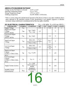
ABSOLUTE MAXIMUM RATINGS*
Voltage on Any Pin Relative to Ground
Operating Temperature Range
Storage Temperature Range
Soldering Temperature
-0.5V to +6.0V
0°C to +70°C
-55°C to +125°C
See IPC/JEDEC J-STD-020A
* This is a stress rating only and functional operation of the device at these or any other conditions above
those indicated in the operation sections of this specification is not implied. Exposure to absolute
maximum rating conditions for extended periods of time may affect reliability.
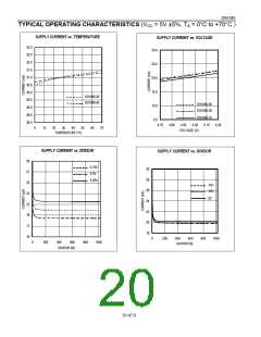
DC ELECTRICAL CHARACTERISTICS
(VCC = 5V ±5%, TA = 0°C to +70°C.)
PARAMETER
SYMBOL CONDITION
MIN
TYP MAX UNITS NOTES
Supply Voltage
VCC
4.75
5
5.25
V
1
High-Level Output
Voltage
IOH = -4mA,
VOH
2.4
V
V
CC = min
(OUT1, OUT0)
Low-Level Output
Voltage
VOL
VIH
IOL = 4mA
0.4
V
V
(OUT1, OUT0)
0.7 x
Vcc
2
SDA, SCL
CTRL0,CTRL1
SDA, SCL
High-Level Input
Voltage
Vcc +
0.3
0.3 x
Vcc
0.8
Low-Level Input
Voltage
VIL
-0.3
V
CTRL0,CTRL1
High-Level Input
Current
IIH
VCC = 5.25V
1
µA
(CTRL1, CTRL0, SDA,
SCL)
Low-Level Input
Current
IIL
VIL = 0
-1
µA
(CTRL1, CTRL0, SDA,
SCL)
CL = 15pF
(both outputs, at
default
Supply Current (Active)
ICC
50
5
mA
mA
frequency)
Power-down
mode
Standby Current
(Power-Down)
ICCQ
16 of 21

 DALLAS [ DALLAS SEMICONDUCTOR ]