DS1085
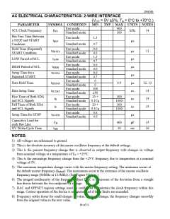
9) This indicates the time taken between power-up and the outputs becoming active. An on-chip delay is
intentionally introduced to allow the oscillator to stabilize. tstab is equivalent to approximately 8000
clock cycles and hence depends on the programmed clock frequency.
10) Output voltage swings can be impaired at high frequencies combined with high-output loading.
11) After this period, the first clock pulse is generated.
12) A device must internally provide a hold time of at least 300ns for the SDA signal (referred to the
V
IH MIN of the SCL signal) in order to bridge the undefined region of the falling edge of SCL.
13) The maximum tHD:DAT need only be met if the device does not stretch the LOW period (tLOW ) of the
SCL signal.
14) A fast-mode device can be used in a standard mode system, but the requirement tSU:DAT > 250ns must
then be met. This is automatically the case if the device does not stretch the LOW period of the SCL
signal. If such a device does stretch the LOW period of the SCL signal, it must output the next data
bit to the SDA line at least tR MAX + tSU:DAT = 1000ns + 250ns = 1250ns before the SCL line is
released.
15) CB—total capacitance of one bus line in picofarads; timing referenced to 0.9VCC and 0.1VCC.
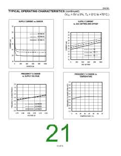
16) EEPROM write begins after a STOP condition occurs.
17) Typical frequency shift due to aging is ±0.5%. Aging stressing includes Level 1 moisture reflow
preconditioning (24hr +125LC bake, 168hr 85LC/85%RH moisture soak, and 3 solder reflow passes
+240 +0/-5LC peak) followed by 1000hr max VCC biased 125LC HTOL, 1000 temperature cycles at -
55LC to +125LC, 96hr 130LC/85%RH/5.5V HAST and 168hr 121LC/2 ATM Steam/Unbiased
Autoclave.
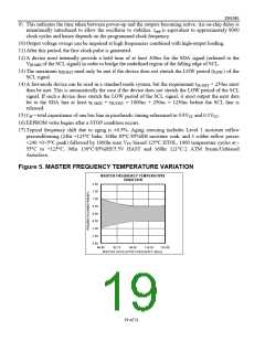
Figure 5. MASTER FREQUENCY TEMPERATURE VARIATION
M A S T E R F R EQ U E N C Y T E M P E R A T U R E
VA R IA T IO N
2.00
1.50
1.00
0.50
0.00
-0.50
-1.00
-1.50
-2.00
66.00
82.75
99.50
116.25
133.00
M A S TE R O S CILLA TO R F RE Q UE NCY (M Hz )
19 of 21

 DALLAS [ DALLAS SEMICONDUCTOR ]