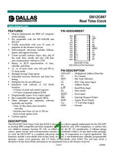
DS12C887
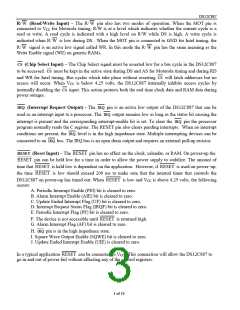
R/ W (Read/Write Input) – The R/ W pin also has two modes of operation. When the MOT pin is
connected to VCC for Motorola timing, R/W is at a level which indicates whether the current cycle is a
read or write. A read cycle is indicated with a high level on R/W while DS is high. A write cycle is
indicated when R/ W is low during DS. When the MOT pin is connected to GND for Intel timing, the
R/ W signal is an active low signal called WR. In this mode the R/ W pin has the same meaning as the
Write Enable signal (WE) on generic RAMs.
CS (Chip Select Input) – The Chip Select signal must be asserted low for a bus cycle in the DS12C887
to be accessed. CS must be kept in the active state during DS and AS for Motorola timing and during RD
and WR for Intel timing. Bus cycles which take place without asserting CS will latch addresses but no
access will occur. When VCC is below 4.25 volts, the DS12C887 internally inhibits access cycles by
internally disabling the CS input. This action protects both the real time clock data and RAM data during
power outages.
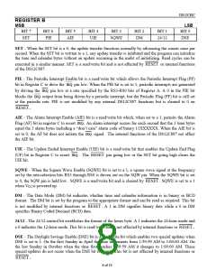
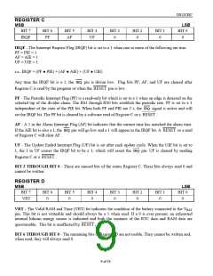
IRQ (Interrupt Request Output) - The IRQ pin is an active low output of the DS12C887 that can be
used as an interrupt input to a processor. The IRQ output remains low as long as the status bit causing the
interrupt is present and the corresponding interrupt-enable bit is set. To clear the IRQ pin the processor
program normally reads the C register. The RESET pin also clears pending interrupts. When no interrupt
conditions are present, the IRQ level is in the high impedance state. Multiple interrupting devices can be
connected to an IRQ bus. The IRQ bus is an open drain output and requires an external pull-up resistor.
RESET (Reset Input) – The RESET pin has no effect on the clock, calendar, or RAM. On power-up the
RESET pin can be held low for a time in order to allow the power supply to stabilize. The amount of
time that RESET is held low is dependent on the application. However, if RESET is used on power–up,
the time RESET is low should exceed 200 ms to make sure that the internal timer that controls the
DS12C887 on power-up has timed out. When RESET is low and VCC is above 4.25 volts, the following
occurs:
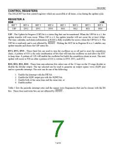
A. Periodic Interrupt Enable (PEI) bit is cleared to zero.
B. Alarm Interrupt Enable (AIE) bit is cleared to zero.
C. Update Ended Interrupt Flag (UF) bit is cleared to zero.
D. Interrupt Request Status Flag (IRQF) bit is cleared to zero.
E. Periodic Interrupt Flag (PF) bit is cleared to zero.
F. The device is not accessible until RESET is returned high.
G. Alarm Interrupt Flag (AF) bit is cleared to zero.
H. IRQ pin is in the high impedance state.
I. Square Wave Output Enable (SQWE) bit is cleared to zero.
J. Update Ended Interrupt Enable (UIE) is cleared to zero.
In a typical application RESET can be connected to VCC . This connection will allow the DS12C887 to
go in and out of power fail without affecting any of the control registers.
3 of 19

 DALLAS [ DALLAS SEMICONDUCTOR ]