DS12C887
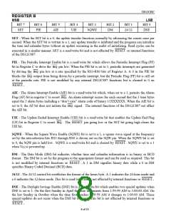
REGISTER B
MSB
LSB
BIT 7
SET
BIT 6
PIE
BIT 5
AIE
BIT 4
UIE
BIT 3
SQWE
BIT 2
DM
BIT 1
24/12
BIT 0
DSE
SET - When the SET bit is a 0, the update transfer functions normally by advancing the counts once per
second. When the SET bit is written to a 1, any update transfer is inhibited and the program can initialize
the time and calendar bytes without an update occurring in the midst of initializing. Read cycles can be
executed in a similar manner. SET is a read/write bit and is not affected by RESET or internal functions
of the DS12C887.
PIE - The Periodic Interrupt Enable bit is a read/write bit which allows the Periodic Interrupt Flag (PF)
bit in Register C to drive the IRQ pin low. When the PIE bit is set to 1, periodic interrupts are generated
by driving the IRQ pin low at a rate specified by the RS3-RS0 bits of Register A. A 0 in the PIE bit
blocks the IRQ output from being driven by a periodic interrupt, but the Periodic Flag (PF) bit is still set
at the periodic rate. PIE is not modified by any internal DS12C887 functions but is cleared to 0 on
RESET .
AIE - The Alarm Interrupt Enable (AIE) bit is a read/write bit which, when set to a 1, permits the Alarm
Flag (AF) bit in register C to assert IRQ . An alarm interrupt occurs for each second that the 3 time bytes
equal the 3 alarm bytes including a “don’t care” alarm code of binary 11XXXXXX. When the AIE bit is
set to 0, the AF bit does not initiate the IRQ signal. The internal functions of the DS12C887 not affect
the AIE bit.
UIE - The Update Ended Interrupt Enable (UIE) bit is a read/write bit that enables the Update End Flag
(UF) bit in Register C to assert IRQ . The RESET pin going low or the SET bit going high clears the
UIE bit.
SQWE - When the Square Wave Enable (SQWE) bit is set to a 1, a square wave signal at the frequency
set by the rate-selection bits RS3 through RS0 is driven out on the SQW pin. When the SQWE bit is set
to 0, the SQW pin is held low. SQWE is a read/write bit and is cleared by RESET . SQWE is set to a 1
when VCC is powered up.
DM - The Data Mode (DM) bit indicates whether time and calendar information is in binary or BCD
format. The DM bit is set by the program to the appropriate format and can be read as required. This bit
is not modified by internal functions or RESET . A 1 in DM signifies binary data while a 0 in DM
specifies Binary Coded Decimal (BCD) data.
24/12 - The 24/12 control bit establishes the format of the hours byte. A 1 indicates the 24-hour mode and
a 0 indicates the 12-hour mode. This bit is read/write and is not affected by internal functions or RESET .
DSE - The Daylight Savings Enable (DSE) bit is a read/write bit which enables two special updates when
DSE is set to 1. On the first Sunday in April the time increments from 1:59:59 AM to 3:00:00 AM. On
the last Sunday in October when the time first reaches 1:59:59 AM it changes to 1:00:00 AM. These
special updates do not occur when the DSE bit is a zero. This bit is not affected by internal functions or
RESET .
8 of 19

 DALLAS [ DALLAS SEMICONDUCTOR ]