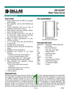
DS12C887
OPERATION
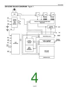
The block diagram in Figure 1 shows the pin connections with the major internal functions of the
DS12C887. The following paragraphs describe the function of each pin.
SIGNAL DESCRIPTIONS
GND, VCC - DC power is provided to the device on these pins. VCC is the +5 volt input. When 5 volts are
applied within normal limits, the device is fully accessible and data can be written and read. When VCC is
below 4.25 volts typical, reads and writes are inhibited. However, the timekeeping function continues
unaffected by the lower input voltage. As VCC falls below 3 volts typical, the RAM and timekeeper are
switched over to an internal lithium energy source. The timekeeping function maintains an accuracy of ±1
minute per month at 25°C regardless of the voltage input on the VCC pin.
MOT (Mode Select) – The MOT pin offers the flexibility to choose between two bus types. When
connected to VCC, Motorola bus timing is selected. When connected to GND or left disconnected, Intel
bus timing is selected. The pin has an internal pull-down resistance of approximately 20KΩ.
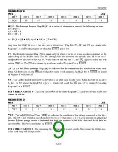
SQW (Square Wave Output) – The SQW pin can output a signal from one of 13 taps provided by the
15 internal divider stages of the Real Time Clock. The frequency of the SQW pin can be changed by
programming Register A as shown in Table 1. The SQW signal can be turned on and off using the SQWE
bit in Register B. The SQW signal is not available when VCC is less than 4.25 volts typical.
AD0-AD7 (Multiplexed Bidirectional Address/Data Bus) – Multiplexed buses save pins because
address information and data information time share the same signal paths. The addresses are present
during the first portion of the bus cycle and the same pins and signal paths are used for data in the second
portion of the cycle. Address/data multiplexing does not slow the access time of the DS12C887 since the
bus change from address to data occurs during the internal RAM access time. Addresses must be valid
prior to the falling edge of AS/ALE, at which time the DS12C887 latches the address from AD0 to AD6.
Valid write data must be present and held stable during the latter portion of the DS or WR pulses. In a
read cycle the DS12C887 outputs 8 bits of data during the latter portion of the DS or RD pulses. The read
cycle is terminated and the bus returns to a high impedance state as DS transitions low in the case of
Motorola timing or as RD transitions high in the case of Intel timing.
AS (Address Strobe Input) – A positive going address strobe pulse serves to demultiplex the bus. The
falling edge of AS/ALE causes the address to be latched within the DS12C887. The next rising edge that
occurs on the AS bus will clear the address regardless of whether CS is asserted. Access commands
should be sent in pairs.
DS (Data Strobe or Read Input) – The DS/RD pin has two modes of operation depending on the level
of the MOT pin. When the MOT pin is connected to VCC, Motorola bus timing is selected. In this mode
DS is a positive pulse during the latter portion of the bus cycle and is called Data Strobe. During read
cycles, DS signifies the time that the DS12C887 is to drive the bidirectional bus. In write cycles the
trailing edge of DS causes the DS12C887 to latch the written data. When the MOT pin is connected to
GND, Intel bus timing is selected. In this mode the DS pin is called Read(RD). RD identifies the time
period when the DS12C887 drives the bus with read data. The RD signal is the same definition as the
Output Enable (OE) signal on a typical memory.
2 of 19

 DALLAS [ DALLAS SEMICONDUCTOR ]