CY8C9520A, CY8C9540A
CY8C9560A
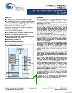
Figure 1. Logical Structure of the IO Port
Architecture
The “Top Level Block Diagram” on page 1 illustrates the device
block diagram. The main blocks include the control unit, PWMs,
EEPROM, and IO ports. The control unit executes commands
received from the I2C bus and transfers data between other bus
devices and the master device.
GPortx
7 Drive Mode
Registers
The on chip EEPROM can be separated conventionally into two
regions. The first region is designed to store data and is available
for byte wide read/writes through the I2C bus. It is possible to
prevent write operations by setting the WD pin to high. All
EEPROM operations can be blocked by configuration register
settings. The second region allows the user to store the port and
PWM default settings using special commands. These defaults
are automatically reloaded and processed after device power on.
Output
Register
DriveMode
Pull-Up
Data
DriveMode
High Z
PWMs
Select PWM
Input Register
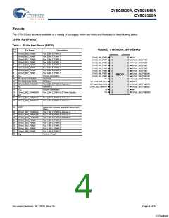
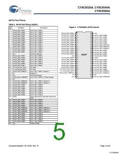
The number of IO lines and PWM sources are listed in table 1.
Table 1. GPIO Availability
Interrupt
Status
Port
CY8C9520A CY8C9540A CY8C9560A
8 Bit IO
GPort 0
GPort 1
GPort 2
GPort 3
GPort 4
GPort 5
GPort 6
GPort 7
PWMs
8 bit
5-8 bita
0-4 bita
8 bit
5-8bita
0-4ita
8 bit
8 bit
4 bit
-
8 bit
5-8 bita
0-4 bita
8 bit
Interrupt
Mask
-
-
Pin Direction
Inversion
8 bit
-
8 bit
-
8 bit
-
-
8 bit
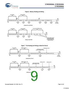
The Port Input and Output registers are separated. When the
Output register is written, the data is sent to the external pins.
When the Input register is read, the external pin logic levels are
captured and transferred. As a result, the read data can be
different from written Output register data. This allows for imple-
mentation of a quasi-bidirectional input-output mode, when the
corresponding binary digit is configured as pulled up/down
output.
4
8
16
a. This port contains configuration-dependant GPIO lines or A1-A6 and WD
lines.
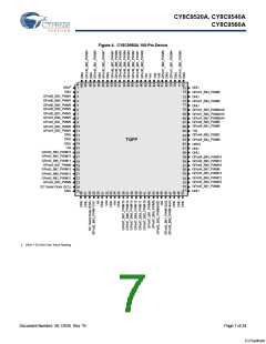
There are four pins on GPort 2 and three on GPort 1 that can be
used as general purpose IO or EEPROM Write Disable (WD) and
I2C-address input (A1-A6), depending on configuration settings.
The figure titled “Logical Structure of the IO Port” shows the
single port logical structure. The Port Drive Mode register gives
the option to select one of seven available modes for each pin
separately: pulled up/down, open drain high/low, strong drive
fast/slow, or high-impedance. By default these configuration
registers store values setting IO pins to pulled up. The Invert
register allows for inversion of the logic of the Input registers
separately for each pin. The Select PWM register assigns pins
as PWM outputs. All of these configuration registers are
read/writable using corresponding commands in the multi-port
device.
Each port has an Interrupt Mask register and an Interrupt Status
register. Each high bit in the Interrupt Status register signals that
there has been a change in the corresponding input line since
the last read of that Interrupt Status register. The Interrupt Status
register is cleared after each read. The Interrupt Mask register
enables/disables activation of the INT line when input levels are
changed. Each high in the Interrupt Mask register masks
(disables) an interrupt generated from the corresponding input
line.
Applications
Each GPIO pin can be used to monitor and control various board
level devices, including LEDs and system intrusion detection
devices.
The on board EEPROM can be used to store information such
as error codes or board manufacturing data for read-back by
application software for diagnostic purposes.
Document Number: 38-12036 Rev. *B
Page 2 of 24
[+] Feedback

 CYPRESS [ CYPRESS ]