PSoC® 3: CY8C32 Family
Data Sheet
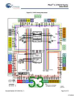
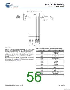
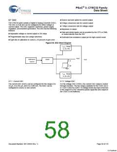
Analog local buses (abus) are routing resources located within
the analog subsystem and are used to route signals between
different analog blocks. There are eight abus routes in CY8C32,
four in the left half (abusl [0:3]) and four in the right half (abusr
[0:3]) as shown in Figure 8-2. Using the abus saves the analog
globals and analog mux buses from being used for
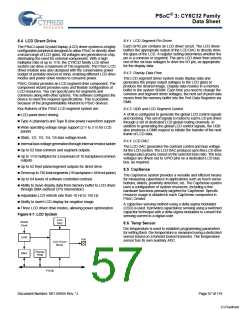
muxes is delivered to the delta-sigma modulator either directly or
through the input buffer. The delta-sigma modulator performs the
actual analog to digital conversion. The modulator over-samples
the input and generates a serial data stream output. This high
speed data stream is not useful for most applications without
some type of post processing, and so is passed to the decimator
through the Analog Interface block. The decimator converts the
high speed serial data stream into parallel ADC results. The
modulator/decimator frequency response is [(sin x)/x]4; a typical
frequency response is shown in Figure 8-5.
interconnecting the analog blocks.
Multiplexers and switches exist on the various buses to direct
signals into and out of the analog blocks. A multiplexer can have
only one connection on at a time, whereas a switch can have
multiple connections on simultaneously. In Figure 8-2,
multiplexers are indicated by grayed ovals and switches are
indicated by transparent ovals.
Figure 8-4. Delta-sigma ADC Block Diagram
Positive
Input Mux
8.2 Delta-sigma ADC
Delta
Sigma
Modulator
Input
Buffer
12 to 20 Bit
Result
Decimator
(Analog Routing)
The CY8C32 device contains one delta-sigma ADC. This ADC
offers differential input, high resolution and excellent linearity,
making it a good ADC choice for measurement applications. The
converter can be configured to output 12-bit resolution at data
rates of up to 192 ksps. At a fixed clock rate, resolution can be
traded for faster data rates as shown in Table 8-1 and Figure 8-3.
Negative
Input Mux
EOC
SOC
Figure 8-5. Delta-sigma ADC Frequency Response,
Normalized to Output, Sample Rate = 48 kHz
Table 8-1. Delta-sigma ADC Performance
MaximumSampleRate
0
-10
-20
-30
-40
-50
-60
-70
-80
-90
-100
Bits
SINAD (dB)
(sps)
192 k
384 k
12
8
66
43
Figure8-3. Delta-sigmaADCSampleRates, Range=±1.024 V
1,000,000
100,000
10,000
100
1,000
10,000
100,000
1,000,000
Input Frequency, Hz
Input frequency, Hz
Resolution and sample rate are controlled by the Decimator.
Data is pipelined in the decimator; the output is a function of the
last four samples. When the input multiplexer is switched, the
output data is not valid until after the fourth sample after the
switch.
1,000
Continuous
Resolution, bits
Mult i-Sample
8.2.2 Operational Modes
100
7
8
9
10
11
12
13
The ADC can be configured by the user to operate in one of four
modes: Single Sample, Multi Sample, Continous, or Multi
Sample (Turbo). All four modes are started by either a write to
the start bit in a control register or an assertion of the Start of
Conversion (SoC) signal. When the conversion is complete, a
status bit is set and the output signal End of Conversion (EoC)
asserts high and remains high until the value is read by either the
DMA controller or the CPU.
8.2.1 Functional Description
The ADC connects and configures three basic components,
input buffer, delta-sigma modulator, and decimator. The basic
block diagram is shown in Figure 8-4. The signal from the input
Document Number: 001-56955 Rev. *J
Page 54 of 119
[+] Feedback

 CYPRESS [ CYPRESS ]