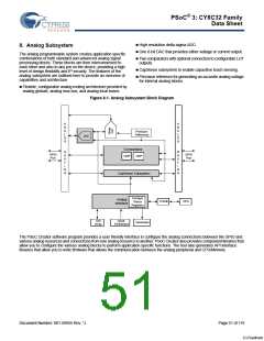
PSoC® 3: CY8C32 Family
Data Sheet
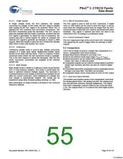
8.2.2.1 Single Sample
8.2.3 Start of Conversion Input
In Single Sample mode, the ADC performs one sample
conversion on a trigger. In this mode, the ADC stays in standby
state waiting for the SoC signal to be asserted. When SoC is
signaled the ADC performs four successive conversions. The
first three conversions prime the decimator. The ADC result is
valid and available after the fourth conversion, at which time the
EoC signal is generated. To detect the end of conversion, the
system may poll a control register for status or configure the
external EoC signal to generate an interrupt or invoke a DMA
request. When the transfer is done the ADC reenters the standby
state where it stays until another SoC event.
The SoC signal is used to start an ADC conversion. A digital
clock or UDB output can be used to drive this input. It can be
used when the sampling period must be longer than the ADC
conversion time or when the ADC must be synchronized to other
hardware. This signal is optional and does not need to be
connected if ADC is running in a continuous mode.
8.2.4 End of Conversion Output
The EoC signal goes high at the end of each ADC conversion.
This signal may be used to trigger either an interrupt or DMA
request.
8.2.2.2 Continuous
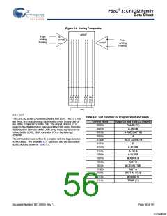
8.3 Comparators
Continuous sample mode is used to take multiple successive
samples of a single input signal. Multiplexing multiple inputs
should not be done with this mode. There is a latency of three
conversion times before the first conversion result is available.
This is the time required to prime the decimator. After the first
result, successive conversions are available at the selected
sample rate.
The CY8C32 family of devices contains two comparators in a
device. Comparators have these features:
Input offset factory trimmed to less than 5 mV
Rail-to-rail common mode input range (VSSA to VDDA
)
Speed and power can be traded off by using one of three
modes: fast, slow, or ultra low-power
Comparator outputs can be routed to lookup tables to perform
simple logic functions and then can also be routed to digital
blocks
The positive input ofthe comparators may be optionally passed
through a low pass filter. Two filters are provided
Comparator inputs can be connections to GPIO or DAC output
8.2.2.3 Multi Sample
Multi sample mode is similar to continuous mode except that the
ADC is reset between samples. This mode is useful when the
input is switched between multiple signals. The decimator is
re-primed between each sample so that previous samples do not
affect the current conversion. Upon completion of a sample, the
next sample is automatically initiated. The results can be
transferred using either firmware polling, interrupt, or DMA.
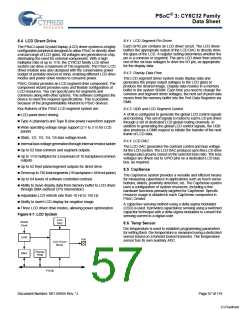
8.3.1 Input and Output Interface
The positive and negative inputs to the comparators come from
the analog global buses, the analog mux line, the analog local
bus and precision reference through multiplexers. The output
from each comparator could be routed to any of the two input
LUTs. The output of that LUT is routed to the UDB Digital System
Interface.
More information on output formats is provided in the Technical
Reference Manual.
Document Number: 001-56955 Rev. *J
Page 55 of 119
[+] Feedback

 CYPRESS [ CYPRESS ]