CY8C24x23 Final Data Sheet
3. Electrical Specifications
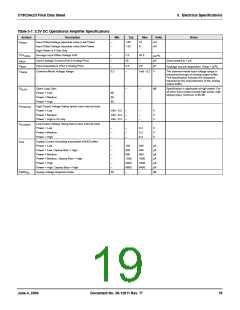
Table 3-7. 3.3V DC Operational Amplifier Specifications
Symbol
Description
Min
Typ
1.65
Max
Units
mV
mV
Notes
V
Input Offset Voltage (absolute value) Low Power
Input Offset Voltage (absolute value) Mid Power
High Power is 5 Volt Only
–
–
10
8
OSOA
1.32
o
TCV
I
Average Input Offset Voltage Drift
Input Leakage Current (Port 0 Analog Pins)
Input Capacitance (Port 0 Analog Pins)
Common Mode Voltage Range
–
7.0
20
4.5
–
35.0
OSOA
µV/ C
–
–
pA
Gross tested to 1 µA.
EBOA
o
C
–
9.5
pF
V
INOA
Package and pin dependent. Temp = 25 C.
V
0.2
Vdd - 0.2
The common-mode input voltage range is
measured through an analog output buffer.
The specification includes the limitations
imposed by the characteristics of the analog
output buffer.
CMOA
G
Open Loop Gain
Power = Low
–
–
dB
Specification is applicable at high power. For
all other bias modes (except high power, high
opamp bias), minimum is 60 dB.
OLOA
OHIGHOA
OLOWOA
SOA
60
60
80
Power = Medium
Power = High
V
V
High Output Voltage Swing (worst case internal load)
Power = Low
Vdd - 0.2
Vdd - 0.2
Vdd - 0.2
–
–
–
–
–
–
V
V
V
Power = Medium
Power = High is 5V only
Low Output Voltage Swing (worst case internal load)
Power = Low
–
–
–
–
–
–
0.2
0.2
0.2
V
V
V
Power = Medium
Power = High
I
Supply Current (including associated AGND buffer)
Power = Low
–
–
–
–
–
–
150
200
µA
µA
µA
µA
µA
µA
Power = Low, Opamp Bias = High
Power = Medium
300
400
600
800
Power = Medium, Opamp Bias = High
Power = High
1200
2400
4600
1600
3200
6400
Power = High, Opamp Bias = High
PSRR
Supply Voltage Rejection Ratio
50
–
–
dB
OA
June 4, 2004
Document No. 38-12011 Rev. *F
19

 CYPRESS [ CYPRESS ]