CY8C24x23 Final Data Sheet
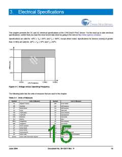
3. Electrical Specifications
3.3
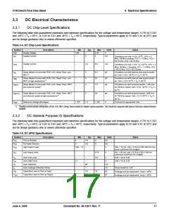
DC Electrical Characteristics
3.3.1
DC Chip-Level Specifications
The following table lists guaranteed maximum and minimum specifications for the voltage and temperature ranges: 4.75V to 5.25V
and -40°C ≤ T ≤ 85°C, or 3.0V to 3.6V and -40°C ≤ T ≤ 85°C, respectively. Typical parameters apply to 5V and 3.3V at 25°C and
A
A
are for design guidance only or unless otherwise specified.
Table 3-4. DC Chip-Level Specifications
Symbol
Description
Min
3.00
Typ
Max
5.25
Units
Notes
Vdd
Supply Voltage
Supply Current
–
5
V
o
I
–
8
mA
DD
Conditions are Vdd = 5.0V, 25 C, CPU = 3
MHz, 48 MHz disabled. VC1 = 1.5 MHz, VC2 =
93.75 kHz, VC3 = 93.75 kHz.
o
I
Supply Current
–
3.3
6.0
mA
DD3
Conditions are Vdd = 3.3V, T = 25 C, CPU = 3
A
MHz, 48 MHz = Disabled, VC1 = 1.5 MHz, VC2
= 93.75 kHz, VC3 = 93.75 kHz.
I
I
I
Sleep (Mode) Current with POR, LVD, Sleep Timer, and
–
–
–
3
4
4
6.5
25
µA
µA
µA
Conditions are with internal slow speed oscilla-
SB
a
o
o
WDT.
tor, Vdd = 3.3V, -40 C <= T <= 55 C.
A
Sleep (Mode) Current with POR, LVD, Sleep Timer, and
Conditions are with internal slow speed oscilla-
SBH
SBXTL
a
o
o
WDT at high temperature.
tor, Vdd = 3.3V, 55 C < T <= 85 C.
A
Sleep (Mode) Current with POR, LVD, Sleep Timer, WDT,
7.5
Conditions are with properly loaded, 1 µW max,
a
o
and external crystal.
32.768 kHz crystal. Vdd = 3.3V, -40 C <= T <=
A
o
55 C.
I
Sleep (Mode) Current with POR, LVD, Sleep Timer, WDT,
–
5
26
µA
Conditions are with properly loaded, 1µW max,
SBXTLH
a
o
and external crystal at high temperature.
32.768 kHz crystal. Vdd = 3.3 V, 55 C < T <=
A
o
85 C.
V
Reference Voltage (Bandgap)
1.275
1.3
1.325
V
Trimmed for appropriate Vdd.
REF
a. Standby current includes all functions (POR, LVD, WDT, Sleep Time) needed for reliable system operation. This should be compared with devices that have similar functions
enabled.
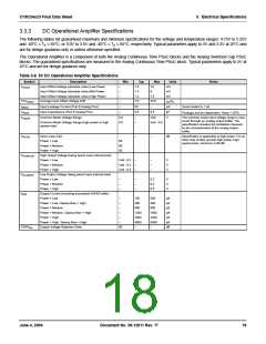
3.3.2
DC General Purpose IO Specifications
The following table lists guaranteed maximum and minimum specifications for the voltage and temperature ranges: 4.75V to 5.25V
and -40°C ≤ T ≤ 85°C, or 3.0V to 3.6V and -40°C ≤ T ≤ 85°C, respectively. Typical parameters apply to 5V and 3.3V at 25°C and
A
A
are for design guidance only or unless otherwise specified.
Table 3-5. DC GPIO Specifications
Symbol
Description
Min
Typ
5.6
Max
Units
kΩ
Notes
R
Pull up Resistor
4
4
8
8
–
PU
PD
OH
R
Pull down Resistor
High Output Level
5.6
–
kΩ
V
Vdd - 1.0
V
IOH = 10 mA, Vdd = 4.75 to 5.25V (80 mA max-
imum combined IOH budget)
V
Low Output Level
–
–
0.75
0.8
V
IOL = 25 mA, Vdd = 4.75 to 5.25V (150 mA
maximum combined IOL budget)
OL
V
V
V
I
Input Low Level
Input High Level
Input Hysterisis
–
–
V
Vdd = 3.0 to 5.25
Vdd = 3.0 to 5.25
IL
IH
H
2.1
–
–
V
60
1
–
mV
nA
pF
pF
Input Leakage (Absolute Value)
Capacitive Load on Pins as Input
Capacitive Load on Pins as Output
–
–
Gross tested to 1 µA.
IL
o
C
C
–
3.5
3.5
10
10
IN
Package and pin dependent. Temp = 25 C.
o
–
OUT
Package and pin dependent. Temp = 25 C.
June 4, 2004
Document No. 38-12011 Rev. *F
17

 CYPRESS [ CYPRESS ]