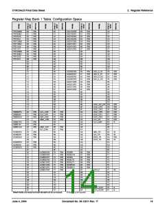
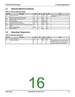
CY8C24x23 Final Data Sheet
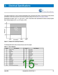
3. Electrical Specifications
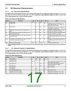
3.3.3
DC Operational Amplifier Specifications
The following tables list guaranteed maximum and minimum specifications for the voltage and temperature ranges: 4.75V to 5.25V
and -40°C ≤ T ≤ 85°C, or 3.0V to 3.6V and -40°C ≤ T ≤ 85°C, respectively. Typical parameters apply to 5V and 3.3V at 25°C and
A
A
are for design guidance only or unless otherwise specified.
The Operational Amplifier is a component of both the Analog Continuous Time PSoC blocks and the Analog Switched Cap PSoC
blocks. The guaranteed specifications are measured in the Analog Continuous Time PSoC block. Typical parameters apply to 5V at
25°C and are for design guidance only.
Table 3-6. 5V DC Operational Amplifier Specifications
Symbol
Description
Min
Typ
1.6
Max
Units
mV
Notes
V
Input Offset Voltage (absolute value) Low Power
Input Offset Voltage (absolute value) Mid Power
Input Offset Voltage (absolute value) High Power
Average Input Offset Voltage Drift
–
–
–
–
10
8
OSOA
1.3
1.2
7.0
mV
mV
7.5
o
TCV
I
35.0
OSOA
µV/ C
Input Leakage Current (Port 0 Analog Pins)
Input Capacitance (Port 0 Analog Pins)
Common Mode Voltage Range
–
–
20
–
pA
Gross tested to 1 µA.
EBOA
o
C
4.5
9.5
pF
V
INOA
Package and pin dependent. Temp = 25 C.
V
0.0
0.5
–
–
Vdd
The common-mode input voltage range is mea-
sured through an analog output buffer. The
specification includes the limitations imposed
by the characteristics of the analog output
buffer.
CMOA
Common Mode Voltage Range (high power or high
opamp bias)
Vdd - 0.5
G
Open Loop Gain
–
–
dB
Specification is applicable at high power. For all
other bias modes (except high power, high
opamp bias), minimum is 60 dB.
OLOA
OHIGHOA
OLOWOA
SOA
Power = Low
60
60
80
Power = Medium
Power = High
V
V
High Output Voltage Swing (worst case internal load)
Power = Low
Vdd - 0.2
Vdd - 0.2
Vdd - 0.5
–
–
–
–
–
–
V
V
V
Power = Medium
Power = High
Low Output Voltage Swing (worst case internal load)
Power = Low
–
–
–
–
–
–
0.2
0.2
0.5
V
V
V
Power = Medium
Power = High
I
Supply Current (including associated AGND buffer)
Power = Low
–
150
300
600
1200
2400
4600
–
200
400
800
1600
3200
6400
–
µA
µA
µA
µA
µA
µA
dB
Power = Low, Opamp Bias = High
Power = Medium
–
–
Power = Medium, Opamp Bias = High
Power = High
–
–
Power = High, Opamp Bias = High
Supply Voltage Rejection Ratio
–
PSRR
60
OA
June 4, 2004
Document No. 38-12011 Rev. *F
18

 CYPRESS [ CYPRESS ]