CY7C68300B/CY7C68301B
CY7C68320/CY7C68321
15.0 PCB Layout Recommendations
The following recommendations should be followed to ensure
reliable high-performance operation.
16.0 Quad Flat Package No Leads (QFN)
Package Design Notes
Electrical contact of the part to the Printed Circuit Board (PCB)
is made by soldering the leads on the bottom surface of the
package to the PCB. Hence, special attention is required to the
heat transfer area below the package to provide a good
thermal bond to the circuit board. A Copper (Cu) fill is to be
designed into the PCB as a thermal pad under the package.
Heat is transferred from the AT2LP through the device’s metal
paddle on the bottom side of the package. Heat from here is
conducted to the PCB at the thermal pad. It is then conducted
from the thermal pad to the PCB inner ground plane by a 5 x
5 array of vias. A via is a plated through-hole in the PCB with
a finished diameter of 13 mil. The QFN’s metal die paddle must
be soldered to the PCB’s thermal pad. Solder mask is placed
on the board top side over each via to resist solder flow into
the via. The mask on the top side also minimizes outgassing
during the solder reflow process.
• At least a four-layer impedance controlled board is required
to maintain signal quality.
• Specify impedance targets (ask your board vendor what
they can achieve).
• To control impedance, maintain uniform trace widths and
trace spacing.
• Tominimizereflectedsignals,minimizethenumberofstubs.
• Connections between the USB connector shell and signal
ground must be done near the USB connector.
• Use bypass/flyback capacitors on VBus near the connector.
• DPLUS and DMINUS trace lengths should be kept to within
2 mm of each other in length, with preferred length of 20 –
30 mm.
• Maintain a solid ground plane under the DPLUS and DMI-
NUS traces. Do not allow the plane to be split under these
traces.
• For a more stable design, do not place vias on the DPLUS
or DMINUS trace routing.
• Isolate the DPLUS and DMINUS traces from all other signal
traces by no less than 10 mm.
• Source for recommendations:
• EZ-USB FX2 PCB Design Recommendations, ht-
tp:///www.cypress.com/cfuploads/sup-
port/app_notes/FX2_PCB.pdf.
• High-speed USB Platform Design Guidelines, ht-
tp://www.usb.org/developers/data/hs_usb_pdg_r1_0.pdf.
For further information on this package design please refer to
the application note Surface Mount Assembly of AMKOR’s
MicroLeadFrame (MLF) Technology. The application note
provides detailed information on board mounting guidelines,
soldering flow, rework process, etc.
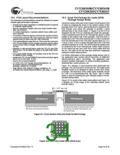
Figure 16-1 displays a cross-sectional area underneath the
package. The cross section is of only one via. The solder paste
template needs to be designed to allow at least 50% solder
coverage. The thickness of the solder paste template should
be 5 mil. It is recommended that “No Clean,” type 3 solder
paste is used for mounting the part. Nitrogen purge is recom-
mended during reflow.
Figure 16-2 is a plot of the solder mask pattern and Figure 16-
3 displays an X-Ray image of the assembly (darker areas
indicate solder.)
0.017” dia
Solder Mask
Cu Fill
Cu Fill
0.013” dia
PCB Material
PCB Material
Via hole for thermally connecting the
This figure only shows the top three layers of the
circuit board: Top Solder, PCB Dielectric, and
the Ground Plane
QFN to the circuit board ground plane.
Figure 16-1. Cross-Section of the Area Under the QFN Package
Figure 16-2. Plot of the Solder Mask (White Area)
Document 38-08033 Rev. *D
Page 34 of 36

 CYPRESS [ CYPRESS ]