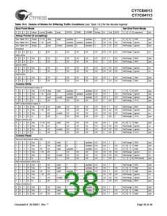
CY7C64013
CY7C64113
21.0
Absolute Maximum Ratings
Storage Temperature ..........................................................................................................................................–65°C to +150°C
Ambient Temperature with Power Applied.................................................................................................................0°C to +70°C
Supply voltage on VCC relative to VSS....................................................................................................................–0.5V to +7.0V
DC Input Voltage........................................................................................................................................... –0.5V to +VCC+0.5V
DC Voltage Applied to Outputs in High Z State ............................................................................................ –0.5V to +VCC+0.5V
Power Dissipation ..............................................................................................................................................................500 mW
Static Discharge Voltage ................................................................................................................................................... >2000V
Latch-up Current ............................................................................................................................................................ >200 mA
Max Output Sink Current into Port 0, 1, 2, 3, and DAC[1:0] Pins ...................................................................................... 60 mA
Max Output Sink Current into DAC[7:2] Pins...................................................................................................................... 10 mA
22.0
Electrical Characteristics
fOSC = 6 MHz; Operating Temperature = 0 to 70°C, VCC = 4.0V to 5.25V
Parameter
General
Conditions
Min.
Max.
Unit
VREF
Vpp
ICC
Reference Voltage
3.3V ±5%
3.15
3.45
0.4
50
50
30
1
V
Programming Voltage (disabled)
VCC Operating Current
–0.4
V
No GPIO source current
mA
µA
mA
µA
ISB1
Iref
Supply Current—Suspend Mode
VREF Operating Current
Note 5
Iil
Input Leakage Current
Any pin
USB Interface
Vdi
Differential Input Sensitivity
Differential Input Common Mode Range
Single Ended Receiver Threshold
Transceiver Capacitance
Hi-Z State Data Line Leakage
External USB Series Resistor
| (D+)–(D–) |
0.2
0.8
0.8
V
V
Vcm
Vse
Cin
2.5
2.0
20
V
pF
µA
Ω
Ilo
0 V < Vin < 3.3 V
–10
10
Rext
RUUP
In series with each USB pin
19
21
External Upstream USB Pull-up Resistor 1.5 kΩ ±5%, D+ to VREG
1.425 1.575
kΩ
Power On Reset
[4]
tvccs
VCC Ramp Rate
USB Upstream
Linear ramp 0V to VCC
0
100
ms
VUOH
VUOL
ZO
Static Output High
15 kΩ ±5% to Gnd
1.5 kΩ ±5% to VREF
Including Rext Resistor
2.8
28
3.6
0.3
44
V
V
Ω
Static Output Low
USB Driver Output Impedance
General Purpose I/O (GPIO)
Pull-up Resistance (typical 14 kΩ)
Input Threshold Voltage
Rup
VITH
VH
8.0
20%
2%
24.0
40%
8%
kΩ
All ports, LOW to HIGH edge
All ports, HIGH to LOW edge
VCC
VCC
Input Hysteresis Voltage
Port 0,1,2,3 Output Low Voltage
VOL
IOL = 3 mA
IOL = 8 mA
0.4
2.0
V
V
VOH
Output High Voltage
IOH = 1.9 mA (all ports 0,1,2,3)
2.4
V
Notes:
4. Power-on Reset occurs whenever the voltage on VCC is below approximately 2.5V.
5. This is based on transitions every 2 full-speed bit times on average.
Document #: 38-08001 Rev. **
Page 41 of 48

 CYPRESS [ CYPRESS ]