CY7C64013
CY7C64113
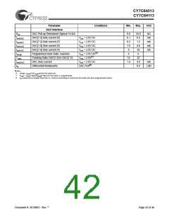
23.0
Switching Characteristics (fOSC = 6.0 MHz)
Parameter
Description
Min.
Max.
Unit
Clock Source
fOSC
tcyc
tCH
tCL
Clock Rate
6 ±0.25%
166.25
MHz
Clock Period
167.08
ns
ns
ns
Clock HIGH time
Clock LOW time
0.45 tCYC
0.45 tCYC
USB Full Speed Signaling[9]
trfs
Transition Rise Time
4
20
20
ns
ns
tffs
Transition Fall Time
4
90
trfmfs
tdratefs
Rise / Fall Time Matching; (tr/tf)
Full Speed Date Rate
111
%
12 ±0.25%
Mb/s
DAC Interface
Current Sink Response Time
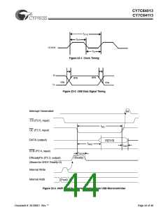
HAPI Read Cycle Timing
tsink
0.8
µs
tRD
Read Pulse Width
15
0
ns
ns
ns
ns
tOED
tOEZ
tOEDR
OE LOW to Data Valid[10, 11]
OE HIGH to Data High-Z[11]
OE LOW to Data_Ready Deasserted[10, 11]
40
20
60
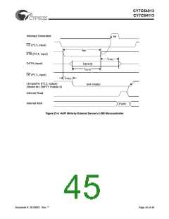
HAPI Write Cycle Timing
tWR
Write Strobe Width
15
5
ns
ns
ns
ns
tDSTB
tSTBZ
tSTBLE
Data Valid to STB HIGH (Data Set-up Time)[11]
STB HIGH to Data High-Z (Data Hold Time)[11]
STB LOW to Latch_Empty Deasserted[10, 11]
Timer Signals
15
0
50
twatch
Watch Dog Timer Period
8.192
14.336
ms
Notes:
9. Per Table 7-6 of revision 1.1 of USB specification.
10. For 25-pF load.
11. Assumes chip select CS is asserted (LOW).
Document #: 38-08001 Rev. **
Page 43 of 48

 CYPRESS [ CYPRESS ]