FOR
FOR
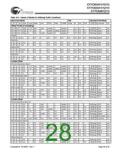
CY7C63411/12/13
CY7C63511/12/13
CY7C63612/13
15.2
Interrupt Latency
Interrupt latency can be calculated from the following equation:
Interrupt Latency = (Number of clock cycles remaining in the current instruction) + (10 clock cycles for the CALL instruction) +
(5 clock cycles for the JMP instruction)
For example, if a 5 clock cycle instruction such as JC is being executed when an interrupt occurs, the first instruction of the
Interrupt Service Routine will execute a min. of 16 clocks (1+10+5) or a max. of 20 clocks (5+10+5) after the interrupt is issued.
Remember that the interrupt latches are sampled at the rising edge of the last clock cycle in the current instruction.
15.2.1 USB Bus Reset Interrupt
The USB Bus Reset interrupt is asserted when a USB bus reset condition is detected. A USB bus reset is indicated by a single
ended zero (SE0) on the upstream port for more than 8 microseconds.
15.2.2 Timer Interrupt
There are two timer interrupts: the 128-µs interrupt and the 1.024-ms interrupt. The user should disable both timer interrupts
before going into the suspend mode to avoid possible conflicts between servicing the interrupts first or the suspend request first.
15.2.3 USB Endpoint Interrupts
There are three USB endpoint interrupts, one per endpoint. The USB endpoints interrupt after the either the USB host or the USB
controller sends a packet to the USB.
15.2.4 DAC Interrupt
Each DAC I/O pin can generate an interrupt, if enabled.The interrupt polarity for each DAC I/O pin is programmable. A positive
polarity is a rising edge input while a negative polarity is a falling edge input. All of the DAC pins share a single interrupt vector,
which means the firmware will need to read the DAC port to determine which pin or pins caused an interrupt.
Please note that if one DAC pin triggered an interrupt, no other DAC pins can cause a DAC interrupt until that pin has returned
to its inactive (non-trigger) state or the corresponding interrupt enable bit is cleared. The USB Controller does not assign interrupt
priority to different DAC pins and the DAC Interrupt Enable Register is not cleared during the interrupt acknowledge process.
15.2.5 GPIO Interrupt
Each of the 32 GPIO pins can generate an interrupt, if enabled. The interrupt polarity can be programmed for each GPIO port as
part of the GPIO configuration. All of the GPIO pins share a single interrupt vector, which means the firmware will need to read
the GPIO ports with enabled interrupts to determine which pin or pins caused an interrupt.
Please note that if one port pin triggered an interrupt, no other port pins can cause a GPIO interrupt until that port pin has returned
to its inactive (non-trigger) state or its corresponding port interrupt enable bit is cleared. The USB Controller does not assign
interrupt priority to different port pins and the Port Interrupt Enable Registers are not cleared during the interrupt acknowledge
process.
Document #: 38-08027 Rev. **
Page 25 of 36

 CYPRESS [ CYPRESS ]