FOR
FOR
CY7C63411/12/13
CY7C63511/12/13
CY7C63612/13
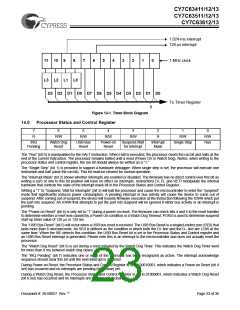
1.024-ms interrupt
128-µs interrupt
11 10
9
8
7
6
5
4
3
2
1
0
1-MHz clock
L3 L2 L1 L0
D3 D2 D1 D0 D7 D6 D5 D4 D3 D2 D1 D0
To Timer Register
8
Figure 13-1. Timer Block Diagram
14.0
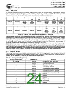
Processor Status and Control Register
7
R
6
5
4
3
2
1
0
R/W
R/W
R/W
R/W
R
R/W
R/W
Run
IRQ
Pending
Watch Dog
Reset
USB Bus
Reset
Power-on
Reset
Suspend,Wait
for Interrupt
Interrupt
Mask
Single Step
The “Run” (bit 0) is manipulated by the HALT instruction. When Halt is executed, the processor clears the run bit and halts at the
end of the current instruction. The processor remains halted until a reset (Power On or Watch Dog). Notice, when writing to the
processor status and control register, the run bit should always be written as a “1.”
The “Single Step” (bit 1) is provided to support a hardware debugger. When single step is set, the processor will execute one
instruction and halt (clear the run bit). This bit must be cleared for normal operation.
The “Interrupt Mask” (bit 2) shows whether interrupts are enabled or disabled. The firmware has no direct control over this bit as
writing a zero or one to this bit position will have no effect on interrupts. Instructions DI, EI, and RETI manipulate the internal
hardware that controls the state of the interrupt mask bit in the Processor Status and Control Register.
Writing a “1” to “Suspend, Wait for Interrupts” (bit 3) will halt the processor and cause the microcontroller to enter the “suspend”
mode that significantly reduces power consumption. A pending interrupt or bus activity will cause the device to come out of
suspend. After coming out of suspend, the device will resume firmware execution at the instruction following the IOWR which put
the part into suspend. An IOWR that attempts to put the part into suspend will be ignored if either bus activity or an interrupt is
pending.
The “Power-on Reset” (bit 4) is only set to “1” during a power on reset. The firmware can check bits 4 and 6 in the reset handler
to determine whether a reset was caused by a Power On condition or a Watch Dog Timeout. PORS is used to determine suspend
start-up timer value of 128 µs or 128 ms.
The “USB Bus Reset” (bit 5) will occur when a USB bus reset is received. The USB Bus Reset is a singled-ended zero (SE0) that
lasts more than 8 microseconds. An SE0 is defined as the condition in which both the D+ line and the D– line are LOW at the
same time. When the SIE detects this condition, the USB Bus Reset bit is set in the Processor Status and Control register and
an USB Bus Reset interrupt is generated. Please note this is an interrupt to the microcontroller and does not actually reset the
processor.
The “Watch Dog Reset” (bit 6) is set during a reset initiated by the Watch Dog Timer. This indicates the Watch Dog Timer went
for more than 8 ms between watch dog clears.
The “IRQ Pending” (bit 7) indicates one or more of the interrupts has been recognized as active. The interrupt acknowledge
sequence should clear this bit until the next interrupt is detected.
During Power-on Reset, the Processor Status and Control Register is set to 00010001, which indicates a Power-on Reset (bit 4
set) has occurred and no interrupts are pending (bit 7 clear) yet.
During a Watch Dog Reset, the Processor Status and Control Register is set to 01000001, which indicates a Watch Dog Reset
(bit 6 set) has occurred and no interrupts are pending (bit 7 clear) yet.
Document #: 38-08027 Rev. **
Page 23 of 36

 CYPRESS [ CYPRESS ]