FOR
FOR
CY7C63411/12/13
CY7C63511/12/13
CY7C63612/13
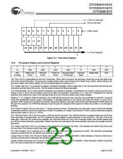
15.0
Interrupts
All interrupts are maskable by the Global Interrupt Enable Register and the USB End Point Interrupt Enable Register. Writing a
“1” to a bit position enables the interrupt associated with that bit position. During a reset, the contents the Global Interrupt Enable
Register and USB End Point Interrupt Enable Register are cleared, effectively disabling all interrupts.
7
6
5
4
3
2
1
0
R/W
R/W
R/W
R/W
R/W
Reserved
Reserved
GPIO
Interrupt
Enable
DAC
Interrupt
Enable
Reserved
1.024-ms
Interrupt
Enable
128-µsec
Interrupt
Enable
USB Bus RST
Interrupt
Enable
7
6
5
4
3
2
1
0
R/W
R/W
R/W
Reserved
Reserved
Reserved
Reserved
Reserved
EPA2
Interrupt
Enable
EPA1
Interrupt
Enable
EPA0
Interrupt
Enable
Figure 15-1. USB End Point Interrupt Enable Register 0x21h (read/write)
Pending interrupt requests are recognized during the last clock cycle of the current instruction. When servicing an interrupt, the
hardware will first disable all interrupts by clearing the Interrupt Enable bit in the Processor Status and Control Register. Next, the
interrupt latch of the current interrupt is cleared. This is followed by a CALL instruction to the ROM address associated with the
interrupt being serviced (i.e., the Interrupt Vector). The instruction in the interrupt table is typically a JMP instruction to the address
of the Interrupt Service Routine (ISR). The user can re-enable interrupts in the interrupt service routine by executing an EI
instruction. Interrupts can be nested to a level limited only by the available stack space.
The Program Counter value as well as the Carry and Zero flags (CF, ZF) are automatically stored onto the Program Stack by the
CALL instruction as part of the interrupt acknowledge process. The user firmware is responsible for insuring that the processor
state is preserved and restored during an interrupt. The PUSH A instruction should be used as the first command in the ISR to
save the accumulator value and the POP A instruction should be used just before the RETI instruction to restore the accumulator
value. The program counter CF and ZF are restored and interrupts are enabled when the RETI instruction is executed.
15.1
Interrupt Vectors
The Interrupt Vectors supported by the USB Controller are listed in Table 15-1. Although Reset is not an interrupt, per se, the first
instruction executed after a reset is at PROM address 0x0000h—which corresponds to the first entry in the Interrupt Vector Table.
Because the JMP instruction is 2 bytes long, the interrupt vectors occupy 2 bytes.
Table 15-1. Interrupt Vector Assignments
Interrupt Vector Number
ROM Address
0x0000h
0x0002h
0x0004h
0x0006h
0x0008h
0x000Ah
0x000Ch
0x000Eh
0x0010h
0x0012h
0x0014h
0x0016h
0x0018h
Function
Execution after Reset begins here
USB Bus Reset interrupt
128-µs timer interrupt
1.024-ms timer interrupt
USB Address A Endpoint 0 interrupt
USB Address A Endpoint 1 interrupt
USB Address A Endpoint 2 interrupt
Reserved
not applicable
1
2
3
4
5
6
7
8
Reserved
9
Reserved
10
11
12
DAC interrupt
GPIO interrupt
Reserved
Document #: 38-08027 Rev. **
Page 24 of 36

 CYPRESS [ CYPRESS ]