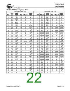
CY7C1361B
CY7C1363B
Current into Outputs (LOW)......................................... 20 mA
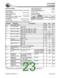
Maximum Ratings
Static Discharge Voltage........................................... >2001V
(Above which the useful life may be impaired. For user guide-
(per MIL-STD-883, Method 3015)
lines, not tested.)
Latch-up Current..................................................... >200 mA
Storage Temperature .................................–65°C to +150°C
Operating Range
Ambient Temperature with
Power Applied.............................................–55°C to +125°C
Ambient
Range
Temperature
VDD
VDDQ
Supply Voltage on VDD Relative to GND........ –0.5V to +4.6V
Commercial 0°C to +70°C 3.3V – 5%/+10% 2.5V – 5%
DC Voltage Applied to Outputs
to VDD
in three-state....................................... –0.5V to VDDQ + 0.5V
Industrial
–40°C to +85°C
DC Input Voltage....................................–0.5V to VDD + 0.5V
Electrical Characteristics Over the Operating Range [12, 13]
Parameter
VDD
VDDQ
Description
Power Supply Voltage
I/O Supply Voltage
Test Conditions
Min.
3.135
3.135
2.375
2.4
Max.
3.6
VDD
Unit
V
V
V
V
V
V
V
V
V
V
V
µA
µA
µA
µA
µA
µA
µA
VDDQ = 3.3V
VDDQ = 2.5V
2.625
VOH
VOL
VIH
VIL
IX
Output HIGH Voltage
Output LOW Voltage
VDDQ = 3.3V, VDD = Min., IOH = –4.0 mA
VDDQ = 2.5V, VDD = Min., IOH = –1.0 mA
VDDQ = 3.3V, VDD = Min., IOL = 8.0 mA
VDDQ = 2.5V, VDD = Min., IOL = 1.0 mA
2.0
0.4
0.4
VDD + 0.3V
VDD + 0.3V
0.8
Input HIGH Voltage[12] VDDQ = 3.3V
VDDQ = 2.5V
2.0
1.7
–0.3
–0.3
–5
Input LOW Voltage[12]
VDDQ = 3.3V
VDDQ = 2.5V
GND ≤ VI ≤ VDDQ
0.7
5
Input Load
Input Current of MODE Input = VSS
Input = VDD
–30
5
Input Current of ZZ
Input = VSS
Input = VDD
–5
–5
30
5
-300
IOZ
IOS
Output Leakage Current GND ≤ VI ≤ VDD, Output Disabled
Output Short Circuit
VDD = Max., VOUT = GND
Current
IDD
VDD Operating Supply VDD = Max., IOUT = 0 mA,
7.5-ns cycle, 133 MHz
8.8-ns cycle, 117 MHz
10-ns cycle, 100 MHz
All speeds
250
220
180
40
mA
mA
Current
f = fMAX = 1/tCYC
ISB1
ISB2
ISB3
Automatic CE
Max. VDD, Device Deselected,
mA
mA
mA
mA
Power-down
VIN ≥ VIH or VIN ≤ VIL, f = fMAX,
Current—TTL Inputs
inputs switching
Automatic CE
Max. VDD, Device Deselected,
All speeds
All speeds
All Speeds
30
40
40
Power-down
V
IN ≥ VDD – 0.3V or VIN ≤ 0.3V,
Current—CMOS Inputs f = 0, inputs static
Automatic CE
Max. VDD, Device Deselected,
Power-down
V
IN ≥ VDDQ – 0.3V or VIN ≤ 0.3V,
Current—CMOS Inputs f = fMAX, inputs switching
ISB4
Automatic CE
Max. VDD, Device Deselected,
IN ≥ VDD – 0.3V or VIN ≤ 0.3V,
f = 0, inputs static
Power-down
V
Current—TTL Inputs
Notes:
12. Overshoot: V (AC) < V +1.5V (Pulse width less than t
/2), undershoot: V (AC) > -2V (Pulse width less than t
/2).
IH
DD
CYC
IL
CYC
13. T
: Assumes a linear ramp from 0v to V (min.) within 200ms. During this time V < V and V
< V
DDQ DD
Power-up
DD
IH
DD
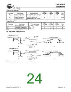
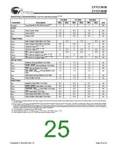
Document #: 38-05302 Rev. *B
Page 23 of 34

 CYPRESS [ CYPRESS ]