CY7C1361B
CY7C1363B
Identification Register Definitions
CY7C1361B
CY7C1363B
(512Kx18)
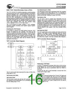
Instruction Field
Revision Number (31:29)
Device Depth (28:24)
(256Kx36)
001
Description
Describes the version number.
Reserved for Internal Use
001
01010
01010
000000
100110
00000110100
1
000000
010110
00000110100
1
Device Width (23:18)
Defines memory type and architecture
Defines width and density
Allows unique identification of SRAM vendor.
Indicates the presence of an ID register.
Cypress Device ID (17:12)
Cypress JEDEC ID Code (11:1)
ID Register Presence Indicator (0)
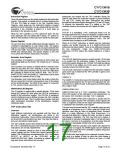
Scan Register Sizes
Register Name
Bit Size (x36)
Bit Size (x18)
Instruction
3
3
Bypass
1
1
ID
32
71
32
71
Boundary Scan Order
Identification Codes
Instruction
Code
Description
000
001
010
EXTEST
Captures I/O ring contents. Places the boundary scan register between TDI and TDO.
Forces all SRAM outputs to High-Z state. This instruction is not 1149.1-compliant.
IDCODE
Loads the ID register with the vendor ID code and places the register between TDI and
TDO. This operation does not affect SRAM operations.
Captures I/O ring contents. Places the boundary scan register between TDI and TDO.
Forces all SRAM output drivers to a High-Z state.
SAMPLE Z
011
100
RESERVED
SAMPLE/PRELOAD
Do Not Use: This instruction is reserved for future use.
Captures I/O ring contents. Places the boundary scan register between TDI and TDO.
Does not affect SRAM operation. This instruction does not implement 1149.1 preload
function and is therefore not 1149.1-compliant.
101
110
111
RESERVED
RESERVED
BYPASS
Do Not Use: This instruction is reserved for future use.
Do Not Use: This instruction is reserved for future use.
Places the bypass register between TDI and TDO. This operation does not affect SRAM
operations.
Document #: 38-05302 Rev. *B
Page 20 of 34

 CYPRESS [ CYPRESS ]