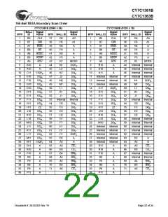
CY7C1361B
CY7C1363B
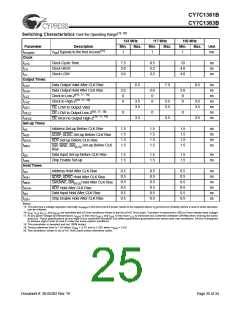
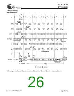
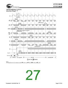
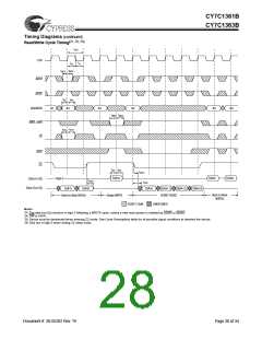
Switching Characteristics Over the Operating Range[19, 20]
133 MHz
117 MHz
100 MHz
Parameter
tPOWER
Clock
tCYC
tCH
tCL
Description
Min.
1
Max.
Min.
1
Max.
Min.
1
Max.
Unit
ms
VDD(Typical) to the first Access[15]
Clock Cycle Time
Clock HIGH
7.5
3.0
3.0
8.5
3.2
3.2
10
4.0
4.0
ns
ns
ns
Clock LOW
Output Times
tCDV
tDOH
tCLZ
tCHZ
tOEV
tOELZ
tOEHZ
Set-up Times
tAS
Data Output Valid After CLK Rise
Data Output Hold After CLK Rise
Clock to Low-Z[16, 17, 18]
6.5
7.5
8.5
ns
ns
ns
ns
ns
ns
ns
2.0
0
0
2.0
0
0
2.0
0
0
Clock to High-Z[16, 17, 18]
3.5
3.5
3.5
3.5
3.5
3.5
OE LOW to Output Valid
OE LOW to Output Low-Z[16, 17, 18]
OE HIGH to Output High-Z[16, 17, 18]
0
0
0
3.5
3.5
3.5
Address Set-up Before CLK Rise
1.5
1.5
1.5
1.5
1.5
1.5
1.5
1.5
1.5
1.5
1.5
1.5
ns
ns
ns
ns
tADS
tADVS
tWES
ADSP, ADSC Set-up Before CLK Rise
ADV Set-up Before CLK Rise
Set-up Before CLK
GW, BWE, BW[A:D]
Rise
tDS
tCES
Data Input Set-up Before CLK Rise
Chip Enable Set-up
1.5
1.5
1.5
1.5
1.5
1.5
ns
ns
Hold Times
tAH
tADH
tWEH
tADVH
tDH
Address Hold After CLK Rise
0.5
0.5
0.5
0.5
0.5
0.5
0.5
0.5
0.5
0.5
0.5
0.5
0.5
0.5
0.5
0.5
0.5
0.5
ns
ns
ns
ns
ns
ns
ADSP, ADSC Hold After CLK Rise
,
,
GW BWE BW[A:D] Hold After CLK Rise
ADV Hold After CLK Rise
Data Input Hold After CLK Rise
Chip Enable Hold After CLK Rise
tCEH
Notes:
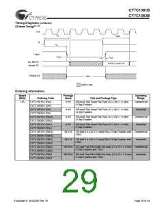
15. This part has a voltage regulator internally; t
can be initiated.
is the time that the power needs to be supplied above V (minimum) initially, before a read or write operation
DD
POWER
16. t
, t
,t
, and t
are specified with AC test conditions shown in part (b) of AC Test Loads. Transition is measured ± 200 mV from steady-state voltage.
CHZ CLZ OELZ
OEHZ
17. At any given voltage and temperature, t
is less than t
and t
is less than t
to eliminate bus contention between SRAMs when sharing the same
CLZ
OEHZ
OELZ
CHZ
data bus. These specifications do not imply a bus contention condition, but reflect parameters guaranteed over worst case user conditions. Device is designed
to achieve High-Z prior to Low-Z under the same system conditions
18. This parameter is sampled and not 100% tested.
19. Timing reference level is 1.5V when V
= 3.3V and is 1.25V when V
= 2.5V.
DDQ
DDQ
20. Test conditions shown in (a) of AC Test Loads unless otherwise noted.
Document #: 38-05302 Rev. *B
Page 25 of 34

 CYPRESS [ CYPRESS ]