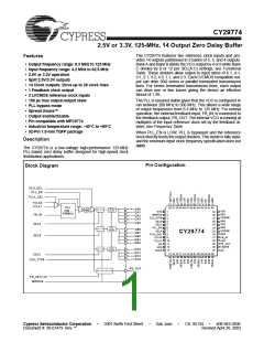
CY29774
DC Electrical Specifications (VDD= 3.3V ± 5%, TA = –40°C to +85°C) (continued)
Parameter
IDDA
Description
PLL Supply Current
Condition
AVDD only
Min.
–
Typ.
5
Max.
Unit
mA
mA
mA
pF
10
1
IDDQ
Quiescent Supply Current
Dynamic Supply Current
Input Pin Capacitance
Output Impedance
All VDD pins except AVDD
–
–
IDD
Outputs loaded @ 100 MHz
–
225
4
–
CIN
–
–
ZOUT
12
15
18
Ω
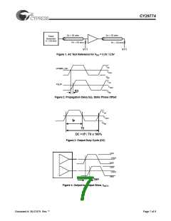
AC Electrical Specifications[6] (VDD= 2.5V ± 5%, TA = –40°C to +85°C)
Parameter Description Condition
fVCO VCO Frequency
Min.
Typ.
Max.
Unit
MHz
MHz
200
25
–
–
–
–
–
–
–
–
–
–
–
–
–
–
–
–
–
–
400
50
fin
Input Frequency
÷8 Feedback
÷12 Feedback
16.6
12.5
8.3
6.3
4.2
0
33.3
25
÷16 Feedback
÷24 Feedback
16.6
12.5
8.3
÷32 Feedback
÷48 Feedback
Bypass mode (PLL_EN = 0)
200
75
frefDC
tr , tf
Input Duty Cycle
25
%
ns
TCLK Input Rise/FallTime
Maximum Output Frequency
0.7V to 1.7V
÷4 Output
–
1.0
fMAX
50
100
50
MHz
÷8 Output
25
÷12 Output
÷16 Output
÷24 Output
16.6
12.5
8.3
45
33.3
25
16.6
55
DC
tr , tf
t(φ)
Output Duty Cycle
%
ns
ps
Output Rise/Fall times
0.7V to 1.8V
0.1
–100
1.0
Propagation Delay (static phase
offset)
TCLK to FB_IN, does not
include jitter
100
tsk(O)
Output-to-Output Skew
Bank-to-Bank Skew
Skew within Bank
–
–
–
–
–
–
–
–
–
–
–
–
150
150
225
10
ps
ps
tsk(B)
Banks at same frequency
Banks at different frequency
–
–
tPLZ, HZ
tPZL, ZH
BW
Output Disable Time
–
ns
ns
Output Enable Time
–
10
PLL Closed Loop Bandwidth (–3 dB)
Cycle-to-Cycle Jitter
0.5 - 1.0
–
MHz
ps
tJIT(CC)
Same frequency
–
–
–
–
–
150
300
100
150
1
Multiple frequencies
tJIT(PER)
tJIT(φ)
Period Jitter
ps
ps
I/O Phase Jitter
tLOCK
Maximum PLL Lock Time
ms
Note:
6. AC characteristics apply for parallel output termination of 50Ω to VTT. Parameters are guaranteed by characterization and are not 100% tested.
Document #: 38-07479 Rev. **
Page 5 of 9

 CYPRESS [ CYPRESS ]