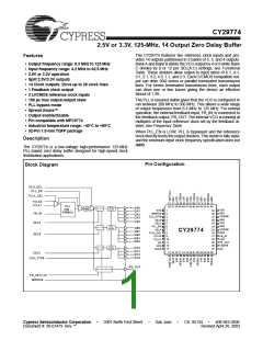
CY29774
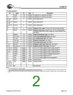
Pin Description[1]
Pin
Name
I/O
I, PD
I, PU
O
Type
Description
9
TCLK0
TCLK1
QA(4:0)
LVCMOS LVCMOS/LVTTL reference clock input
LVCMOS LVCMOS/LVTTL reference clock input
LVCMOS Clock output bank A
10
16, 18, 21,
23, 25
32, 34, 36,
38, 40
QB(4:0)
QC(3:0)
O
O
LVCMOS Clock output bank B
LVCMOS Clock output bank C
44, 46, 48,
50
29
31
FB_OUT
FB_IN
O
LVCMOS Feedback clock output. Connect to FB_IN for normal operation.
I, PU
LVCMOS Feedback clock input. Connect to FB_OUT for normal operation.
This input should be at the same voltage rail as input reference clock.
See Table 1.
2
MR#/OE
CLK_STP#
PLL_EN
TCLK_SEL
VCO_SEL
SEL(A:C)
FB_SEL(1,0)
VDDQA
VDDQB
VDDQC
VDDFB
AVDD
I, PU
I, PU
LVCMOS Output enable/disable input. See Table 2.
LVCMOS Clock stop enable/disable input. See Table 2.
LVCMOS PLL enable/disable input. See Table 2.
LVCMOS Reference select input. See Table 2.
3
6
I, PU
8
I, PD
52
I, PD
LVCMOS VCO divider select input. See Table 2.
LVCMOS Frequency select input, Bank (A:C). See Table 3.
LVCMOS Feedback dividers select input. See Table 4.
7, 4, 5
20, 14
17, 22, 26
33, 37, 41
45, 49
28
I, PD
I, PD
Supply
Supply
Supply
Supply
Supply
Supply
Supply
Supply
VDD
VDD
2.5V or 3.3V Power supply for bank A output clocks[2,3]
2.5V or 3.3V Power supply for bank B output clocks[2,3]
2.5V or 3.3V Power supply for bank C output clocks[2,3]
2.5V or 3.3V Power supply for feedback output clock[2,3]
2.5V or 3.3V Power supply for PLL[2,3]
VDD
VDD
13
VDD
12
VDD
VDD
2.5V or 3.3V Power supply for core and inputs[2,3]
15
AVSS
Ground
Ground
Analog Ground
1, 19, 24,
30, 35, 39,
43, 47, 51
VSS
Common Ground
11, 27, 42
NC
No Connection
Notes:
1. PU = Internal pull up, PD = Internal pull down
2. A 0.1-µF bypass capacitor should be placed as close as possible to each positive power pin (<0.2”). If these bypass capacitors are not close to the pins their
high frequency filtering characteristics will be cancelled by the lead inductance of the traces.
3. AVDD and VDD pins must be connected to a power supply level that is at least equal or higher than that of VDDQA, VDDQB, VDDQC, and VDDFB power supply
pins.
Document #: 38-07479 Rev. **
Page 2 of 9

 CYPRESS [ CYPRESS ]