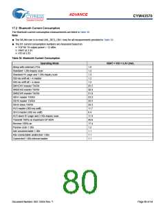
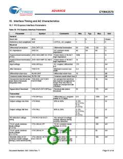
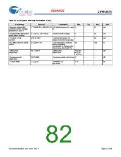
ADVANCE
CYW43570
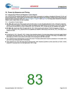
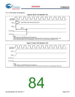
19.1.2 Control Signal Timing Diagrams
Figure 26. WLAN = ON, Bluetooth = ON
32.678 kHz
Sleep Clock
High is 90% of VBAT and low is 10% of VBAT.
VBAT*
VDDIO
100 ms
WL_REG_ON
BT_REG_ON
*Notes:
1. VBAT should not rise 10%–90% faster than 40 microseconds.
2. VBAT should be up before or at the same time as VDDIO. VDDIO should NOT be present first or be held high before VBAT is high.
3. Reset control signal timing for warm boot (high/low/high on REG_ON) is 100 ms and for cold power-on (low/high) is 10 ms.
Figure 27. WLAN = OFF, Bluetooth = OFF
32.678 kHz
Sleep Clock
VBAT*
VDDIO
WL_REG_ON
BT_REG_ON
*Notes:
1. VBAT should not rise 10%–90% faster than 40 microseconds.
2. VBAT should be up before or at the same time as VDDIO. VDDIO should NOT be present first or be held high before VBAT is high.
Document Number: 002-15054 Rev. *I
Page 84 of 94

 CYPRESS [ CYPRESS ]