ADVANCE
CYW43570
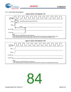
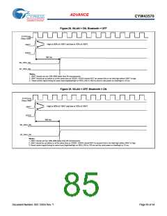
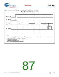
19. Power-Up Sequence and Timing
19.1 Sequencing of Reset and Regulator Control Signals
The CYW43570 has two signals that allow the host to control power consumption by enabling or disabling the Bluetooth, WLAN, and
internal regulator blocks. These signals are described below. Additionally, diagrams are provided to indicate proper sequencing of the
signals for various operational states (see Figure 26, Figure 27, Figure 28 and Figure 29). The timing values indicated are minimum
required values; longer delays are also acceptable.
19.1.1 Description of Control Signals
■ WL_REG_ON: Used by the PMU to power up the WLAN section. It is also OR-gated with the BT_REG_ON input to control the
internal CYW43570 regulators. When this pin is high, the regulators are enabled and the WLAN section is out of reset. When this
pin is low the WLAN section is in reset. If both the BT_REG_ON and WL_REG_ON pins are low, the regulators are disabled.
■ BT_REG_ON: Used by the PMU (OR-gated with WL_REG_ON) to power up the internal CYW43570 regulators. If both the
BT_REG_ON and WL_REG_ON pins are low, the regulators are disabled. When this pin is low and WL_REG_ON is high, the BT
section is in reset.
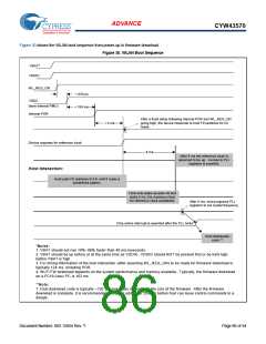
Note:
■ For both the WL_REG_ON and BT_REG_ON pins, there should be at least a 10 ms time delay between consecutive toggles (where
both signals have been driven low). This is to allow time for the CBUCK regulator to discharge. If this delay is not followed, then
there may be a VDDIO in-rush current on the order of 36 mA during the next PMU cold start.
■ The CYW43570 has an internal power-on reset (POR) circuit. The device will be held in reset for a maximum of 110 ms after VDDC
and VDDIO have both passed the POR threshold.
■ VBAT should not rise 10%–90% faster than 40 microseconds. VBAT should be up before or at the same time as VDDIO. VDDIO
should NOT be present first or be held high before VBAT is high.
Document Number: 002-15054 Rev. *I
Page 83 of 94

 CYPRESS [ CYPRESS ]