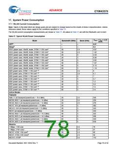
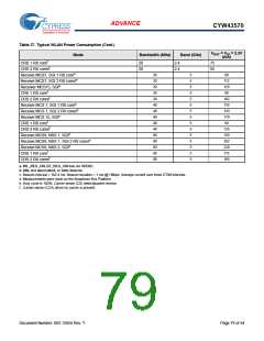
ADVANCE
CYW43570
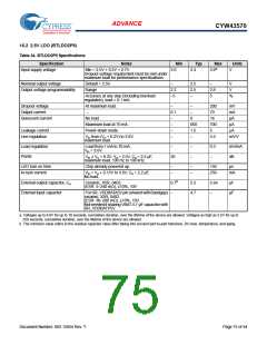
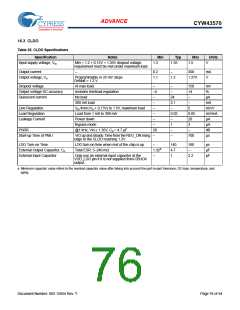
16.3 CLDO
Table 35. CLDO Specifications
Specification
Notes
Min
1.3
Typ
1.35
Max
1.5
Units
Input supply voltage, Vin
Min = 1.2 + 0.15V = 1.35V dropout voltage
requirement must be met under maximum load.
V
Output current
–
0.2
1.1
–
300
mA
V
Output voltage, Vo
Programmable in 25 mV steps.
Default = 1.2.V
1.2
1.275
Dropout voltage
At max load
–
–
150
+4
–
mV
%
Output voltage DC accuracy
Quiescent current
Includes line/load regulation
No load
–4
–
–
24
2.1
–
μA
300 mA load
–
–
mA
mV/V
mV/mA
μA
Line Regulation
Load Regulation
Leakage Current
Vin from (Vo + 0.15V) to 1.5V, maximum load
–
5
Load from 1 mA to 300 mA
Power down
–
0.02
–
0.05
20
3
–
Bypass mode
–
1
μA
PSRR
@1 kHz, Vin ≥ 1.35V, Co = 4.7 μF
20
–
–
dB
Start-up Time of PMU
VIO up and steady. Time from the REG_ON rising –
edge to the CLDO reaching 1.2V.
–
700
μs
LDO Turn-on Time
LDO turn-on time when rest of the chip is up
–
140
4.7
1
180
–
μs
μF
μF
External Output Capacitor, Co
External Input Capacitor
Total ESR: 5–240 mΩ
1.32a
Only use an external input capacitor at the
VDD_LDO pin if it is not supplied from CBUCK
output.
–
2.2
a. Minimum capacitor value refers to the residual capacitor value after taking into account the part-to-part tolerance, DC-bias, temperature, and
aging.
Document Number: 002-15054 Rev. *I
Page 76 of 94

 CYPRESS [ CYPRESS ]