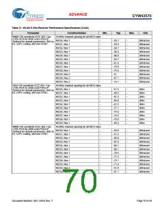
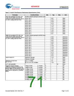
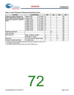
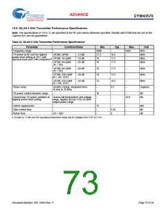
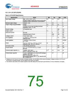
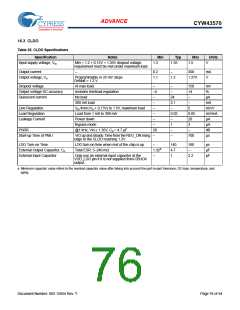
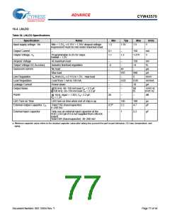
ADVANCE
CYW43570
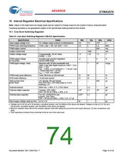
16. Internal Regulator Electrical Specifications
Note: Values in this data sheet are design goals and are subject to change based on the results of device characterization.
Functional operation is not guaranteed outside of the specification limits provided in this section.
16.1 Core Buck Switching Regulator
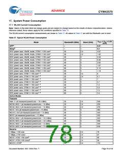
Table 33. Core Buck Switching Regulator (CBUCK) Specifications
Specification
Input supply voltage (DC)
PWM mode switching frequency
PWM output current
Notes
Min
3.0
Typ
3.3
Max
3.6a
Units
DC voltage range inclusive of disturbances.
V
CCM, Load > 100 mA VBAT = 3.6V
2.8
–
4
5.2
600
–
MHz
mA
mA
V
–
–
–
Output current limit
–
1400
1.35
Output voltage range
Programmable, 30 mV steps
Default = 1.35V
1.2
1.5
PWM output voltage
DC accuracy
Includes load and line regulation.
Forced PWM mode
–4
–
–
7
4
%
PWM ripple voltage, static
Measure with 20 MHz bandwidth limit.
Static Load. Max Ripple based on VBAT = 3.6V,
Vout = 1.35V,
20
mVpp
Fsw = 4 MHz, 2.2 μH inductor L > 1.05 μH, Cap
+ Board total-ESR < 20 mΩ,
Cout > 1.9 μF, ESL<200pH
PWM mode peak efficiency
PFM mode efficiency
Peak Efficiency at 200 mA load
10 mA load current
78
70
–
86
81
–
–
%
%
μs
–
Start-up time from
power down
VIO already ON and steady.
Time from REG_ON rising edge to CLDO
reaching 1.2V
850
External inductor
0806 size, ± 30%, 0.11 ± 25% Ohms
–
2.0b
2.2
4.7
–
10c
μH
μF
External output capacitor
Ceramic, X5R, 0402,
ESR <30 mΩ at 4 MHz, ± 20%, 6.3V
External input capacitor
For SR_VDDBATP5V pin,
0.67b
4.7
–
μF
ceramic, X5R, 0603,
ESR < 30 mΩ at 4 MHz, ± 20%, 6.3V, 4.7 μF
Input supply voltage ramp-up time 0V to 3.3V
40
–
–
μs
a. Voltages up to 6.0V for up to 10 seconds, cumulative duration, over the lifetime of the device are allowed. Voltages as high as 5.5V for up to
250 seconds, cumulative duration, over the lifetime of the device are allowed.
b. Minimum capacitor value refers to the residual capacitor value after taking into account the part-to-part tolerance, DC-bias, temperature, and
aging.
c. Total capacitance includes those connected at the far end of the active load.
Document Number: 002-15054 Rev. *I
Page 74 of 94

 CYPRESS [ CYPRESS ]