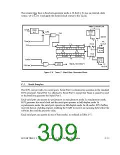
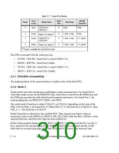
Table C-7. Serial Port Modes
Sync/
Async
Data
Bits
9th Bit
Function
Mode
Baud Clock
CLK24/4 or
Start/Stop
0
Sync
8
None
None
CLK24/12
1
1
1
2
Async
8
9
1 start, 1 stop
1 start, 1 stop
None
Timer 1 or Timer 2
Async CLK24/32 or
CLK24/64
0, 1, parity
3
Async
9
1 start, 1 stop
0, 1, parity
Timer 1 or Timer 2
(1)
Timer 2 available for Serial Port 0 only.
The SFRs associated with the serial ports are:
•
•
•
•
SCON0 - SFR 98h - Serial Port 0 control (Table C-8.).
SBUF0 - SFR 99h - Serial Port 0 buffer.
SCON1 - SFR C0h - Serial Port 1 control (Table C-9.).
SBUF1 - SFR C1h - Serial Port 1 buffer.
C.3.1 803x/805x Compatibility
The implementation of the serial interface is similar to that of the Intel 8052.
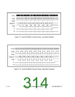
C.3.2 Mode 0
Serial mode 0 provides synchronous, half-duplex serial communication. For Serial Port 0,
serial data output occurs on the RXD0OUT pin, serial data is received on the RXD0 pin, and
the TXD0 pin provides the shift clock for both transmit and receive. For Serial Port 1, the
corresponding pins are RXD1OUT, RXD1, and TXD1.
The serial mode 0 baud rate is either CLK24/12 or CLK24/4, depending on the state of the
SM2_0 bit (or SM2_1 for Serial Port 1). When SM2_0 = 0, the baud rate is CLK24/12, when
SM2_0 = 1, the baud rate is CLK24/4.
Mode 0 operation is identical to the standard 8051. Data transmission begins when an
instruction writes to the SBUF0 (or SBUF1) SFR. The UART shifts the data, LSB first, at the
selected baud rate, until the 8-bit value has been shifted out.
Mode 0 data reception begins when the REN_0 (or REN_1) bit is set and the RI_0 (or RI_1)
bit is cleared in the corresponding SCON SFR. The shift clock is activated and the UART
shifts data in on each rising edge of the shift clock until 8 bits have been received. One
C - 14
Appendix C: 8051 Hardware Description
EZ-USB TRM v1.9

 CYPRESS [ CYPRESS ]