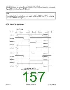
The timing choices for fast write pulses (FWR#) are shown in Figure 8-11. The 8051 can
extend the output data and widths of these pulses by setting cycle stretch values greater
than zero in the 8051 Clock Control Register CKCON (at SFR location 0x8E). The top
five waveforms show the fastest write timings, with a stretch value of 000, which per-
forms the write in eight 8051 clocks. The bottom five waveforms show the same wave-
forms with a stretch value of 001.
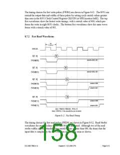
8.7.2 Fast Read Waveforms
tCL
41.66 ns
OSC24
D[7..0]
In
stretch=000, 001
stretch=000, 001
FRD#[00]
D[7..0]
In
FRD#[01]
D[7..0]
In
stretch=000
stretch=001
FRD#[10]
FRD#[10]
D[7..0]
In
stretch=000
stretch=001
FRD#[11]
FRD#[11]
[nn] = RMOD1:RMOD0, RPOL=0
Note: If WPOL=1 the waveforms are inverted
Figure 8-12. Fast Read Timing
The timing choices for fast read pulses (FRD#) are shown in Figure 8-12. Read Strobe
waveforms for stretch values of 000 and 001 are indicated. Although two of the read
strobe widths can be extended using stretch values greater than 000, the times that the
input data is sampled by the EZ-USB core remains the same as shown.
EZ-USB TRM v1.9
Chapter 8. EZ-USB CPU
Page 8-13

 CYPRESS [ CYPRESS ]