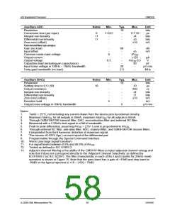
AIS Baseband Processor
CMX910
7.
Performance Specification
7.1
Electrical Performance
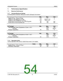
7.1.1 Absolute Maximum Ratings
Exceeding these maximum ratings can result in damage to the device.
Min.
Max.
4.5
IOVDD + 0.3
AVDD + 0.3
+30
Unit
V
V
Supply (IOVDD - AVSS or DVSS
)
-0.3
-0.3
-0.3
-30
Voltage on any digital pin to DVSS
Voltage on any analogue pin to AVSS
Current into or out of IOVDD, AVSS and DVSS pins
Current into or out of any other pin
mA
mA
-20
+20
Q1 Package
Total Allowable Power Dissipation at Tamb = 25°C
... Derating
Min.
Max.
3500
35.0
Unit
mW
mW/°C
°C
Storage Temperature
-55
+125
L9 Package
Min.
Max.
1690
16.9
Unit
mW
mW/°C
°C
Total Allowable Power Dissipation at Tamb = 25°C
... Derating
Storage Temperature
-55
+125
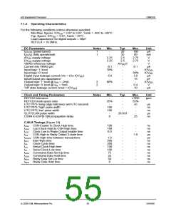
7.1.2 Operating Limits
Correct operation of the device outside these limits is not implied.
Notes
Min.
3.00
-40
Max.
3.60
+85
Unit
V
°C
Supply (IOVDD – AVSS or DVSS
Operating Temperature
)
© 2009 CML Microsystems Plc
54
D/910/6

 CMLMICRO [ CML MICROCIRCUITS ]