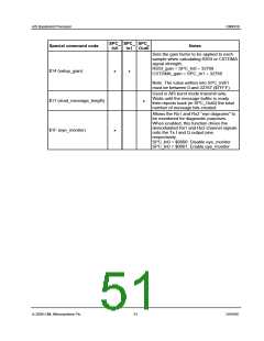
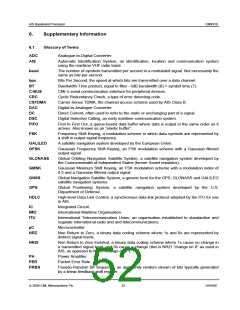
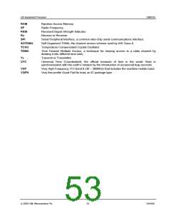
AIS Baseband Processor
CMX910
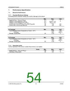
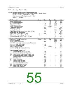
7.1.3 Operating Characteristics
For the following conditions unless otherwise specified:
Min./Max. figures: IOVDD = 3.0V to 3.6V, Tamb = -40C to +85°C.
Typ. figures: IOVDD = 3.3V, Tamb = 25°C.
Load capacitance for digital outputs = 30pF.
REFCLK = 19.2MHz.
DC Parameters
IIOVDD (powersaved)
IIOVDD (fully operational)
AVDD supply voltage
DVDD supply voltage
Notes
Min.
-
-
2.25
2.25
Typ.
20
35
2.5
Max.
100
60
2.75
2.75
Unit
µA
mA
V
1
1
2.5
V
VBIAS reference voltage
Current into VBIAS pin
Input logic ‘1’ level
AVDD/2
V
µA
IOVDD
IOVDD
µA
pF
IOVDD
V
-0.1
70%
-
-5.0
-
80%
-
-
-
-
-
-
-
-
-
-
0.1
-
30%
5.0
15
-
Input logic ‘0’ level
Digital input leakage current (Vin = 0 to IOVDD
Input/Output pin capacitance
Output logic ‘1’ level @ IOH = -2mA
Output logic ‘0’ level @ IOL = 3mA
)
2
2
0.4
10
'Off' state leakage current (Vout = IOVDD
)
µA
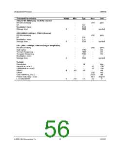
Clock and Timing Parameters
REFCLK tolerance
REFCLK mark:space ratio
UTC1PPS rising edge tolerance (wrt UTC second)
UTC1PPS ‘high’ pulse width
UTC1PPS ‘low’ pulse width
Notes
Min.
Typ.
-
-
-
-
-
Max.
±TBD
65%
±5
-
-
-
25
Unit
ppm
-
35%
-
100
100
-
µs
ns
ns
µs
ns
SLOTCLKN pulse width
CSXN to EXP[0-5]N propagation delay
20.833
-
0
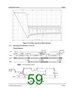
C-BUS Timings (Figure 16)
tCSE CSN-Enable to Clock-High time
tCSH Last Clock-High to CSN-High time
100
100
0.0
-
1.0
200
200
100
100
75
-
-
-
-
-
-
-
-
-
-
-
-
-
-
-
-
ns
ns
ns
µs
µs
ns
ns
ns
ns
ns
ns
ns
ns
tLOZ
tHIZ
Clock-Low to Reply Output enable time
CSN-High to Reply Output 3-state time
1.0
tCSOFF CSN-High time between transactions
tNXT Inter-Byte time
-
-
-
-
-
-
-
-
-
tCK
tCH
tCL
Clock-Cycle time
Serial Clock-High time
Serial Clock-Low time
tCDS Command Data Set-Up time
tCDH Command Data Hold time
tRDS Reply Data Set-Up time
tRDH Reply Data Hold time
25
50
0
© 2009 CML Microsystems Plc
55
D/910/6

 CMLMICRO [ CML MICROCIRCUITS ]