AIS Baseband Processor
CMX910
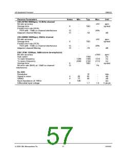
Auxiliary ADC
Resolution
Conversion time (per input)
Integral non-linearity
Differential non-linearity
Zero error (offset)
Notes
Min.
-
11.021
Typ.
10
-
-
-
Max.
-
117.35
±4
±3
±10
Unit
bits
µs
bits
bits
mV
9
11
11
-
-
-
-
Uncommitted op-amps:
Gain (no load)
Input offset
Common mode input voltage
Output current
Output voltage
Capacitive load (including pin capacitance)
Input noise voltage in 100Hz – 10kHz bandwidth
Unity-gain bandwidth (no load)
-
-
0
-
0.5
-
-
60
-
-
-
-
-
±5
AVDD
±125
dB
mV
µA
V
pF
µV rms
MHz
AVDD-0.5
-
30
-
-
20
2.5
-
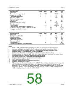
Auxiliary DACs
Resolution
Settling time to 0.5 LSB
Output resistance
Integral non-linearity
Differential non-linearity
Zero error (offset)
Notes
Min.
-
Typ.
10
Max.
-
Unit
bits
µs
10
10
250
±4
±1
±10
-
-
-
-
-
5
-
-
-
-
-
Ω
bits
bits
mV
Resistive load
Output noise voltage in 30kHz bandwidth
kΩ
µV rms
-
5
-
Notes:
1.
Tamb = 25°C, not including any current drawn from the device pins by external circuitry.
2.
3.
4.
Maximum total IOL for all outputs is 50mA, maximum total IOH for all outputs is 50mA.
Through G(M)FSK/FSK transmit filter, DAC, reconstruction filter and external RC filter.
Measured with a 2.25kHz test signal in a 9kHz bandwidth.
5.
Peak to peak differential, assuming AVDD = 2.5V. Level is proportional to AVDD.
6.
7.
Through external RC filter, anti-alias filter, ADC, channel filter, and G(M)FSK/FSK receive filters.
Extrapolated from third harmonic distortion at maximum signal.
8.
This means ±0.425V (typ.) on each input of the differential pair.
9.
Programmable through the Special Command Interface.
10.
11.
12.
13.
Worst case large signal transition.
For signal levels between 0.5% and 99.5% of AVDD.
Tested as defined in IEC 61993-2.
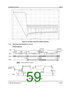
Adjacent channel filtering is the ability of the CMX910 filters to reject adjacent channel energy and
note that it does not correspond directly to the ‘Adjacent Channel Selectivity’ as defined by
IEC61993-2 (or IEC 62287). The filter characteristic in each of the I and Q paths for 25kHz mode
operation is shown in Figure 15. Note that the pass-band has a gain of +10dB and stop band is
-60dB so the typical rejection is +10 – (-60) = 70dB
.
© 2009 CML Microsystems Plc
58
D/910/6

 CMLMICRO [ CML MICROCIRCUITS ]