Baseband Processor For Mixed Mode Land Mobile Radio
CMX880
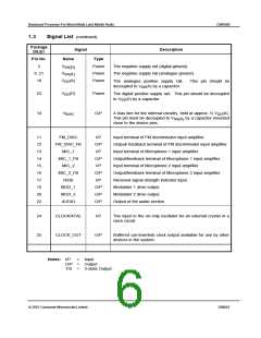
1.3
Signal List (continued)
Package
Signal
Description
D6,E1
Pin No.
5
Name
VSS(D)
VSS(A)
VDD(A)
Type
Power
Power
Power
The negative supply rail (digital ground).
The negative supply rail (analogue ground).
9, 21
18
The analogue positive supply rail.
decoupled to VSS(A) by a capacitor.
This pin should be
23
10
VDD(D)
Power
O/P
The digital positive supply rail. This pin should be decoupled
to VSS(D) by a capacitor.
VBIAS
A bias line for the internal circuitry, held at approx. ½ VDD(A).
This pin must be decoupled to VSS(A) by a capacitor mounted
close to the device pins.
11
12
13
14
15
16
17
19
20
22
FM_DISC
FM_DISC_FB
MIC_1
I/P
O/P
I/P
Input terminal of FM discriminator input amplifier.
Output/ feedback terminal of FM discriminator input amplifier.
Input terminal of Microphone 1 input amplifier.
Output/feedback terminal of Microphone 1 input amplifier.
Input terminal of Microphone 2 input amplifier.
Output/feedback terminal of Microphone 2 input amplifier.
Received signal strength indicator input.
Modulator 1 drive output.
MIC_1_FB
MIC_2
O/P
I/P
MIC_2_FB
RSSI
O/P
I/P
MOD_1
O/P
O/P
O/P
MOD_2
Modulator 2 drive output.
AUDIO
Output of the audio section.
24
25
CLOCK/XTAL
CLOCK_OUT
I/P
The input to the on-chip oscillator for an external crystal or a
clock circuit.
O/P
Buffered (un-inverted) clock output available for use by other
devices in the system.
Notes: I/P
=
=
=
Input
Output
3-state Output
O/P
T/S
ã 2001 Consumer Microcircuits Limited
6
D/880/1

 CMLMICRO [ CML MICROCIRCUITS ]