Baseband Processor For Mixed Mode Land Mobile Radio
CMX880
CONTENTS
Section
Page
1.0
1.1
1.2
1.3
1.4
1.5
Features and Applications .......................................................................................... 1
Brief Description......................................................................................................... 1
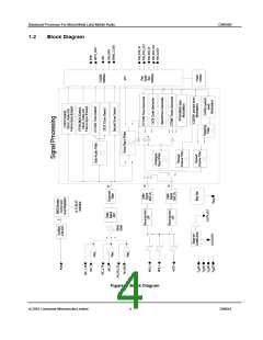
Block Diagram............................................................................................................. 4
Signal List................................................................................................................... 5
External Components.................................................................................................. 7
General Description.................................................................................................. 10
1.5.1 Operation...................................................................................................... 11
1.5.1.1 Sleep Mode....................................................................................... 11
1.5.1.2 RSSI Monitoring ............................................................................... 12
1.5.1.3 Receive Mode ................................................................................... 13
1.5.1.4 Transmit Mode.................................................................................. 27
1.5.1.5 Configuration Options...................................................................... 37
1.5.1.6 “C-BUS” Operation........................................................................... 39
1.5.1.7 Fast Serial Bus Operation ................................................................ 40
1.5.2 Software Description.................................................................................... 41
1.5.2.1 “C-BUS” Register Description.......................................................... 41
1.5.2.2 FSB Register Description ................................................................. 65
Application Notes...................................................................................................... 67
Performance Specification........................................................................................ 68
1.7.1 Electrical Performance ................................................................................. 68
1.7.2 Packaging..................................................................................................... 80
1.6
1.7
Table
Page
Table 1 Suggested Routing of Data...................................................................................... 13
Table 2 CTCSS Rx Tone Programming................................................................................. 16
Table 3 Selcall Tone Sets and Corresponding Rx Programming Codes............................... 17
Table 4 DCS Modulation Modes ........................................................................................... 19
Table 5 DCS 23 Bit Codes..................................................................................................... 20
Table 6 Frame Sync Pattern ................................................................................................. 22
Table 7 Symbol Word Encoding........................................................................................... 22
Table 8 Data Frequencies For Each Baud Rate .................................................................... 25
Table 9 Concurrent Tx Modes Supported by the CMX880 .................................................... 27
Table 10 CTCSS TX Tone Programming............................................................................... 30
Table 11 Selcall Tone Sets and Corresponding Tx Programming Codes ............................. 31
Table 12 DTMF Tone Pairs and Corresponding Tx Programming Codes.............................. 32
Table 13 C4FM Symbol Word Encoding ............................................................................... 33
Table 14 I and Q Level Encoding.......................................................................................... 34
Table 15 Receive and Transmit Path Configurations. .......................................................... 37
Table 16 Gain, Path Selection And Power Save Options..................................................... 38
Table 17 Maximum Data Transfer Latency ........................................................................... 39
Table 18 PROGRAMMING REGISTER Functions Summary................................................... 58
ã 2001 Consumer Microcircuits Limited
2
D/880/1

 CMLMICRO [ CML MICROCIRCUITS ]