Baseband Processor For Mixed Mode Land Mobile Radio
CMX880
Figure
Page
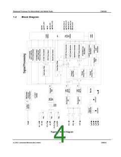
Figure 1 Block Diagram.......................................................................................................... 4
Figure 2 Recommended External Components...................................................................... 7
Figure 3 Power Supply Connections and De-coupling........................................................... 8
Figure 4 Modulator output components to achieve -100dB/decade roll-off .......................... 9
Figure 5 Analogue Channel, RX Audio Filter Frequency Response...................................... 14
Figure 6 De-emphasis Curve for TIA/EIA-603 Compliance ................................................... 14
Figure 7 Low Pass Sub-Audio Band Filter for CTCSS and DCS ........................................... 15
Figure 8 The 4-Level Symbols, Unfiltered and RC Filtered................................................... 21
Figure 9 Receiver Filter Frequency Response...................................................................... 21
Figure 10 Filter Characteristics for Decoded C4FM Voice Signals....................................... 23
Figure 11 Modulating Waveforms for 1200 and 2400 Baud FFSK Signals............................ 25
Figure 12 25kHz Channel Audio Filter Response Template.................................................. 28
Figure 13 12.5kHz Channel Audio Filter Response Template............................................... 28
Figure 14 Audio Frequency Pre-emphasis Template............................................................ 29
Figure 15 C4FM Transmitter Processing Path...................................................................... 33
Figure 16 CQPSK Transmitter Processing Path................................................................... 35
Figure 17 Voice Filter Template for C4FM and CQPSK Transmission.................................. 35
Figure 18 Power-Save Blocks............................................................................................... 37
Figure 19 “C-BUS” Protocol................................................................................................. 39
Figure 20 Fast Serial Bus Data Transfer Protocol................................................................ 40
Figure 21 SNR vs Nominal C4FM Frame Sync Cross-Correlation Peak................................ 52
Figure 22 Possible APCO 25 Configuration.......................................................................... 67
Figure 23 “C-BUS” Timing.................................................................................................... 76
Figure 24 Fast Serial Bus Timings. ...................................................................................... 77
Figure 25 Typical FFSK/MSK Bit Error Rate Graph ............................................................... 78
Figure 26 FFSK/MSK Typical Variation of Bit Error Rate with Input Signal Level................ 78
Figure 27 Typical Bit Error Rate with and without FEC........................................................ 79
Figure 28 Mechanical Outline of 28-pin SSOP (D6): Order as part no. CMX880D6............. 80
Figure 29 Mechanical Outline of 28-pin TSSOP (E1): Order as part no. CMX880E1............ 80
Note: This product is in development: Changes and additions will be made to this
specification. Items marked TBD or left blank will be included in later issues.
Information in this data sheet should not be relied upon for final product design.
ã 2001 Consumer Microcircuits Limited
3
D/880/1

 CMLMICRO [ CML MICROCIRCUITS ]