Baseband Processor For Mixed Mode Land Mobile Radio
CMX880
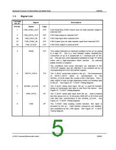
1.3
Signal List
Package
Signal
Description
D6, E1
Pin No.
1
Name
Type
FSB_SYNC_OUT
O/P
Fast Serial Bus (FSB) Frame Sync for data transfer output to
external DSP.
2
FSB_DATA_OUT
FSB_DATA_IN
FSB_SYNC_IN
FSB_CLOCK
O/P
I/P
FSB Data output to external DSP.
26
27
28
FSB Data input from external DSP.
O/P
O/P
FSB Frame Sync for data transfer input from external DSP.
FSB Clock output to external DSP.
3
IRQN
O/P
This output indicates an interrupt condition to the µC by going
to a logic "0". This is a "wire-ORable" output, enabling the
connection of up to 8 peripherals to 1 interrupt port on the
µC. This pin has a low impedance pulldown to logic "0" when
active and a high-impedance when inactive. An external
pullup resistor is required.
The conditions that cause interrupts are indicated in the
‘STATUS’ register and are effective if not masked out by a
corresponding bit in the IRQ MASK register.
4
REPLY_DATA
T/S
The “C-BUS” serial data output to the µC. The transmission
of
REPLY_DATA
bytes
is
synchronised
to
the
SERIAL_CLOCK under the control of the CSN input. This 3-
state output is held at high impedance when not sending data
to the µC. See Figure 23 “C-BUS” Timing diagram.
6
7
SERIAL_CLOCK
CMD_DATA
I/P
I/P
The “C-BUS” serial clock input the µC, is used for transfer
timing of commands and data to and from the device. See
Figure 23 “C-BUS” Timing diagram.
The “C-BUS” serial data input from the µC. Data is loaded
into this device in 8 or 16-bit words, MSB (B7 or B15) first and
LSB (B0) last, synchronised to the SERIAL_CLOCK. See
Figure 23 “C-BUS” Timing diagram.
8
CSN
I/P
The “C-BUS” data loading control function: this input is
provided by the µC. Data transfer sequences are initiated,
and completed by the CSN signal. See Figure 23 “C-BUS”
Timing diagram.
ã 2001 Consumer Microcircuits Limited
5
D/880/1

 CMLMICRO [ CML MICROCIRCUITS ]