AX.25 Modem
CMX7031/CMX7041
Monitor
Input1 Gain: $B1:b12-10
Output1
Input1
DISC
ALT
Fixed – 0dB
Fine Gain: $C2:b3-0
MOD1
Mux
Mux
Tx Signal Processing
Rx Signal Processing
$B1:
b9-6
$B1:
b5-2
Coarse Gain: $C2:b6-4
Fine Gain: $C2:b11-8
MIC
MOD2
Output2
Coarse Gain: $C2:b14-12
Figure 19 Level Adjustments
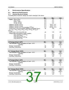
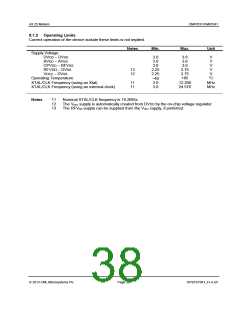
7.12.1 Transmit Path Levels
For the maximum signal out of the MOD1 and MOD2 attenuators, the signal level at the output of the
Analogue Routing block should not exceed +8.69dB, assuming both fine and coarse output attenuators
are set to a gain of 0dB.
7.12.2 Receive Path Levels
The Input Gain adjustment has a variable gain of up to +22.4dB and no attenuation. If the highest gain
setting were used, then the maximum allowable input signal level at the DISCFB pin would be 12.0mV
rms. With the lowest gain setting (0dB), the maximum allowable input signal level at the DISCFB pin
would be +8.69dB (838mVrms) which is an absolute maximum, which should not be exceeded anywhere
in the signal processing chain if severe distortion is to be avoided.
2013 CML Microsystems Plc
Page 34
D/7031/7041_FI-4.x/5

 CMLMICRO [ CML MICROCIRCUITS ]