CS49300 Family DSP
EXTMEM serves as the active low chip select
output.
always places the most significant address bits first
(see Figures 30, 31, and 32 for details).
Pin
Number
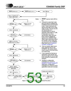
It should be noted that there are currently no
applications for the CS493XX that use more than
32 kilobytes of external memory (RAM or ROM),
which corresponds to only 15 address lines.
Pin Name
/EMOE
Pin Description
* External Memory Output Enable
& Address Latch Strobe
* External Memory Write Strobe
External Memory Select
Address and Data Bit 7
Address and Data Bit 6
Address and Data Bit 5
Address and Data Bit 4
Address and Data Bit 3
Address and Data Bit 2
Address and Data Bit 1
Address and Data Bit 0
5
/EMWR
/EXTMEM
EMAD7
EMAD6
EMAD5
EMAD4
EMAD3
EMAD2
EMAD1
EMAD0
4
21
8
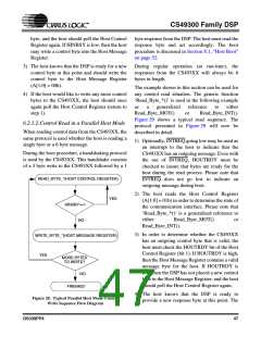
7.1. Non-Paged Memory
9
Non-paged memories can be used for autobooting
a single piece of full download application code
such as MP3, HDCD, or SRS Circle Surround. A
non-paged memory architecture should be used in
systems which will need to access a single dsp
application code image (32 Kilobyte maximum),
which means that only 15 bits would be required to
access the entire application code image. The 16th
address bit coming from the DSP should be left
unconnected. Figure 35 shows the functional
timing of an autoboot sequence in which three
address cycles are illustrated.
10
11
14
15
16
17
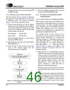
* - These pins must be configured appropriately to select a se-
rial host communication mode for the CS493XX at the rising
edge of RESET
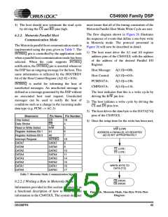
Table 8. Memory Interface Pins
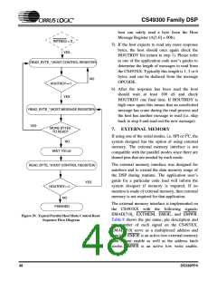
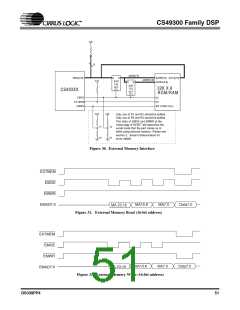
Figure 30, "External Memory Interface" on page
51 illustrates one possible external memory
architecture for the CS493XX. Figure 31,
"External Memory Read (16-bit address)" on page
The DSP always considers its address space to
51 shows the functional timing of a 16 bit address range from 0x0000 to 0xFFFF. This means that the
memory read and Figure 32, "External Memory
Write (16-bit address)" on page 51 shows the
decoder is unaware of any data which falls outside
of this 64 Kilobyte range. When the DSP is
functional timing of a 16 bit address memory write. performing an autoboot, the process always begins
It should be noted that this memory example gives
the DSP visibility to up to 64 kilobytes of memory.
with address 0x0000. This means that the host
microcontroller must be involved in memory
accesses which exceed the 32 Kilobyte scope of the
CS493XX, and the host must also manage access to
all pieces of autoboot code which do not physically
reside at location 0x0000. The limitations of a non-
paged memory are easily seen, and they can be
circumvented using paged memory designs as
discussed in the next section.
The external memory address is capable of
addressing up to 16 megabytes total through a 24
bit addressing scheme. The address comes from the
DSP writing three initial bytes of address
consecutively on EMAD[7:0]. Each byte of
address is externally latched with the rising edge of
EMOE while EXTMEM is high. After the 3-byte
address is latched externally, the CS493XX then
drives EXTMEM and EMOE low simultaneously
to select the external memory. During this time the
data is read by the CS493XX.
7.2. Paged Memory
Sometimes it is desirable for the external memory
to be paged by the host controller. One application
where this is useful is the autoboot mechanism
(discussed in Section 8.2, “Autoboot” on page 56).
Using paged memory allows multiple dsp firmware
applications to be stored in the same memory, with
To extend the example shown in Figures 30 to 32
to allow for a 24-bit address, the system designer
would add another latch to the system. The DSP
DS339PP4
49

 CIRRUS [ CIRRUS LOGIC ]