CS4397
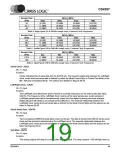
Sample Rate
(kHz)
MCLK (MHz)
256x
384x
512x
768x
32
44.1
48
8.1920
11.2896
12.2880
12.2880
16.9344
18.4320
16.3840
22.5792
24.5760
24.5760
33.8688
36.8640
Table 4. Single Speed (16 to 50 kHz sample rates) Common Clock Frequencies
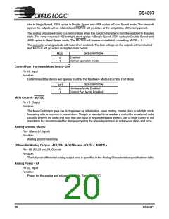
Sample Rate MCLK (MHz)
(kHz)
64
88.2
96
128x
192x
256x
384x
8.1920
11.2896
12.2880
12.2880
16.9344
18.4320
16.3840
22.5792
24.5760
24.5760
33.8688
36.8640
Table 5. Double Speed (50 to 100 kHz sample rates) Common Clock Frequencies
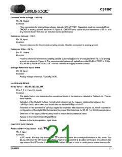
Sample Rate MCLK (MHz)
(kHz)
176.4
192
64x
11.2896
12.2880
96x
16.9344
18.4320
128x
22.5792
24.5760
192x
33.8688
36.8640
Table 6. Quad Speed (100 to 200 kHz sample rates) Common Clock Frequencies
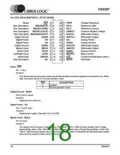
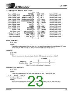
Serial Clock - SCLK
Pin 11, Input
Function:
Clocks individual bits of serial data into the SDATA pin. The required relationship between the Left/Right
clock, serial clock and serial data is defined by either the Mode Control Byte in Control Port Mode or the
M0 - M4 pins in Hardware Mode. The options are detailed in Figures 29-33
Left/Right Clock - LRCK
Pin 12, Input
Function:
The Left/Right clock determines which channel is currently being input on the serial audio data input,
SDATA. The frequency of the Left/Right clock must be at the input sample rate. Audio samples in
Left/Right sample pairs will be simultaneously output from the digital-to-analog converter whereas
Right/Left pairs will exhibit a one sample period difference. The required relationship between the
Left/Right clock, serial clock and serial data is defined by the Mode Control Byte and the options are de-
tailed in Figures 29-33
Serial Audio Data - SDATA
Pin 13, Input
Function:
Two's complement MSB-first serial data is input on this pin. The data is clocked into SDATA via the serial
clock and the channel is determined by the Left/Right clock. The required relationship between the
Left/Right clock, serial clock and serial data is defined by the Mode Control Byte and the options are de-
tailed inin Figures 29-33
Soft Mute - MUTE
Pin 15, Input
Function:
The analog outputs will ramp to a muted state when enabled. The ramp requires 1152 left/right clock cy-
DS333F1
19

 CIRRUS [ CIRRUS LOGIC ]